Ordering information, Timing diagrams – Cypress CY7C1365C User Manual
Page 16

CY7C1365C
Document #: 38-05690 Rev. *E
Page 16 of 18
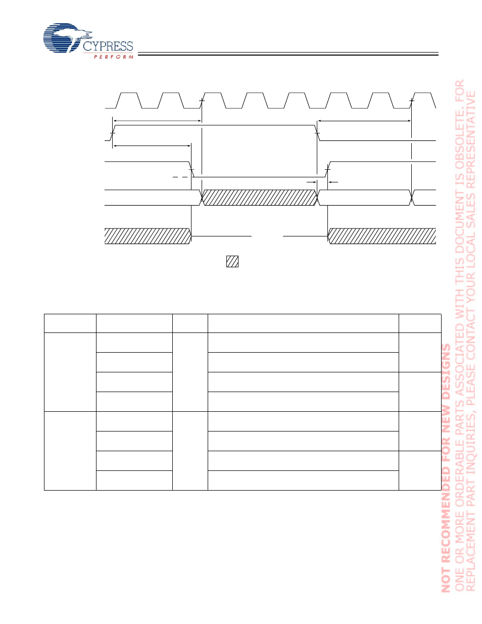
ZZ Mode Timing
[21, 22]
Ordering Information
Not all of the speed, package and temperature ranges are available. Please contact your local sales representative or
visit
www.cypress.com
for actual products offered.
Speed
(MHz)
Ordering Code
Package
Diagram
Package Type
Operating
Range
133
CY7C1365C-133AXC
51-85050 100-pin Thin Quad Flat Pack (14 x 20 x 1.4 mm) Lead-Free
(3 Chip Enable)
Commercial
CY7C1365C-133AJXC
100-pin Thin Quad Flat Pack (14 x 20 x 1.4 mm) Lead-Free
(2 Chip Enable)
CY7C1365C-133AXI
100-pin Thin Quad Flat Pack (14 x 20 x 1.4 mm) Lead-Free
(3 Chip Enable)
Industrial
CY7C1365C-133AJXI
100-pin Thin Quad Flat Pack (14 x 20 x 1.4 mm) Lead-Free
(2 Chip Enable)
100
CY7C1365C-100AXC
51-85050 100-pin Thin Quad Flat Pack (14 x 20 x 1.4 mm) Lead-Free
(3 Chip Enable)
Commercial
CY7C1365C-100AJXC
100-pin Thin Quad Flat Pack (14 x 20 x 1.4 mm) Lead-Free
(2 Chip Enable)
CY7C1365C-100AXI
100-pin Thin Quad Flat Pack (14 x 20 x 1.4 mm) Lead-Free
(3 Chip Enable)
Industrial
CY7C1365C-100AJXI
100-pin Thin Quad Flat Pack (14 x 20 x 1.4 mm) Lead-Free
(2 Chip Enable)
Notes:
21. Device must be deselected when entering ZZ mode. See Cycle Descriptions table for all possible signal conditions to deselect the device.
22. DQs are in High-Z when exiting ZZ sleep mode.
Timing Diagrams
(continued)
t
ZZ
I
SUPPLY
CLK
ZZ
t
ZZREC
ALL INPUTS
(except ZZ)
DON’T CARE
I
DDZZ
t
ZZI
t
RZZI
Outputs (Q)
High-Z
DESELECT or READ Only
