Timing diagrams – Cypress CY7C1365C User Manual
Page 14
CY7C1365C
Document #: 38-05690 Rev. *E
Page 14 of 18
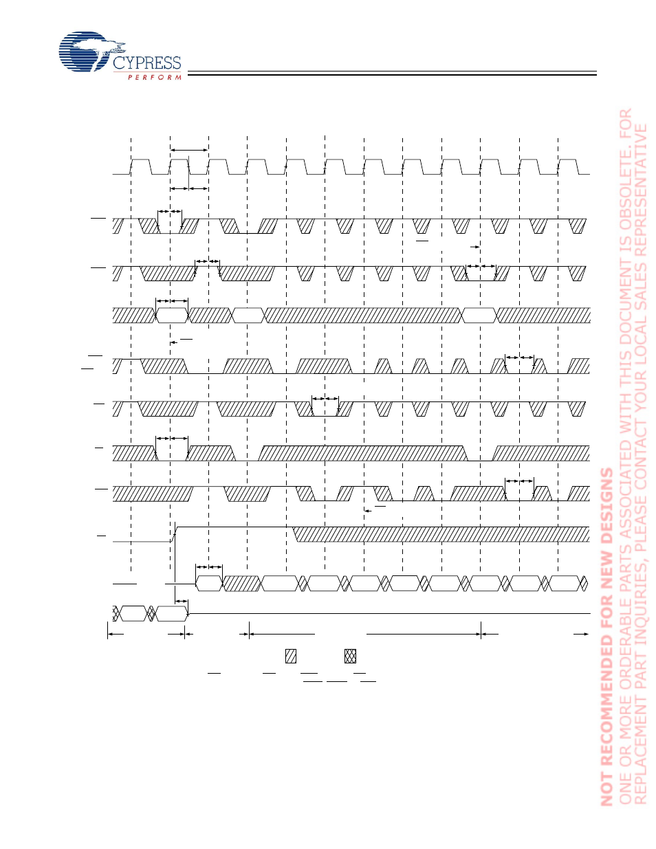
Write Cycle Timing
[18, 19]
Notes:
18. Full width write can be initiated by either GW LOW; or by GW HIGH, BWE LOW and BW[A:D] LOW.
19. The data bus (Q) remains in High-Z following a Write cycle unless an ADSP, ADSC, or ADV cycle is performed.
Timing Diagrams
(continued)
tCYC
t
CL
CLK
tADH
tADS
ADDRESS
t
CH
tAH
tAS
A1
tCEH
tCES
High-Z
BURST READ
BURST WRITE
D(A2)
D(A2 + 1)
D(A2 + 1)
D(A1)
D(A3)
D(A3 + 1)
D(A3 + 2)
D(A2 + 3)
A2
A3
Extended BURST WRITE
D(A2 + 2)
Single WRITE
tADH
tADS
tADH
tADS
t
OEHZ
tADVH
tADVS
tWEH
tWES
t
DH
t
DS
t
WEH
t
WES
Byte write signals are ignored for first cycle when
ADSP initiates burst.
ADSC extends burst.
ADV suspends burst.
DON’T CARE
UNDEFINED
ADSP
ADSC
BWE,
BW
[A:D]
GW
CE
ADV
OE
Data in (D)
Data Out (Q)
See also other documents in the category Cypress Hardware:
- CY7C1410AV18 (29 pages)
- CY7C1411JV18 (28 pages)
- CY7C1383FV25 (28 pages)
- CY14B256L (18 pages)
- CY7C1307BV25 (21 pages)
- CY7C1041DV33 (13 pages)
- CY62167EV18 (13 pages)
- Perform CY7C1565V18 (28 pages)
- STK11C68-5 (15 pages)
- 7C185-20 (11 pages)
- CY7C1168V18 (27 pages)
- CY7C1318CV18-250BZC (26 pages)
- CY7C1364C (18 pages)
- Perform CY7C1382D (34 pages)
- CY7C106D (11 pages)
- CY14E102N (21 pages)
- CY7C1418AV18 (31 pages)
- enCoRe CY7C638xx (83 pages)
- CY7C1018DV33 (9 pages)
- CY7C1292DV18 (23 pages)
- CY7C130 (19 pages)
- CY7C1424BV18 (30 pages)
- CY62157EV18 (12 pages)
- CY7C1392BV18 (31 pages)
- CY7C1302DV25 (18 pages)
- Perform CY7C1511KV18 (31 pages)
- West Bridge Astoria AN46860 (4 pages)
- CY7C1386FV25 (30 pages)
- CY7C1163V18 (29 pages)
- CY7C1266V18 (27 pages)
- CY7C1334H (13 pages)
- CY7C1018CV33 (7 pages)
- CY62136VN (12 pages)
- AN20639 (3 pages)
- CY7C1338G (17 pages)
- CY7C1462AV33 (27 pages)
- CY7C1145V18 (28 pages)
- STK11C88 (15 pages)
- CY7C1231H (12 pages)
- Perform CY7C142 (15 pages)
- CY14E256L (18 pages)
- STK15C88 (15 pages)
- CY7C1297H (15 pages)
- CY7C1441AV33 (31 pages)
- CapSense CY8C20x36 (34 pages)