Capacitance, Ac test loads and waveforms, Data retention characteristics – Cypress CY62157CV33 User Manual
Page 5: Data retention waveform
CY62157CV30/33
Document #: 38-05014 Rev. *F
Page 5 of 13
Capacitance
[7]
Parameter
Description
Test Conditions
Max.
Unit
C
IN
Input Capacitance
T
A
= 25°C, f = 1 MHz,
V
CC
= V
CC(typ.)
6
pF
C
OUT
Output Capacitance
8
pF
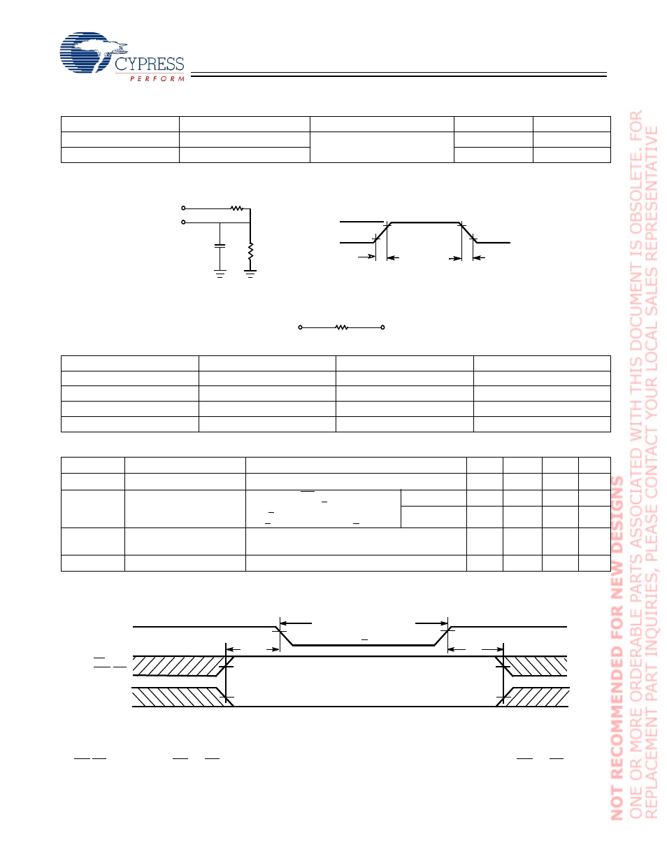
AC Test Loads and Waveforms
V
CC
Typ
V
CC
OUTPUT
R2
30 pF
INCLUDING
JIG AND
SCOPE
GND
90%
10%
90%
10%
OUTPUT
V
TH
Equivalent to:
THÉVENIN EQUIVALENT
ALL INPUT PULSES
R
TH
R1
Rise TIme: 1 V/ns
Fall Time: 1 V/ns
Parameters
3.0V
3.3V
Unit
R1
1.105
1.216
ΚΩ
R2
1.550
1.374
ΚΩ
R
TH
0.645
0.645
ΚΩ
V
TH
1.75
1.75
V
Data Retention Characteristics
(Over the Operating Range)
Parameter
Description
Conditions
Min.
Typ.
[2]
Max.
Unit
V
DR
V
CC
for Data Retention
1.5
V
I
CCDR
Data Retention Current
V
CC
= 1.5V, CE
1
> V
CC
– 0.2V or
CE
2
< 0.2V,
V
IN
> V
CC
– 0.2V or V
IN
< 0.2V
Auto-A
4
20
µA
Auto-E
4
60
µA
t
CDR
[8]
Chip Deselect to Data
Retention Time
0
ns
t
R
[8]
Operation Recovery Time
t
RC
ns
Data Retention Waveform
[9]
Notes:
8. Full Device AC operation requires linear V
CC
ramp from V
DR
to V
CC(min.)
> 100
µs or stable at V
CC(min.)
>100
µs.
9. BHE.BLE is the AND of both BHE and BLE. Chip can be deselected by either disabling the chip enable signals or by disabling both BHE and BLE.
V
CC(min.)
V
CC(min.)
t
CDR
V
DR
> 1.5 V
DATA RETENTION MODE
t
R
CE
1
or
V
CC
BHE.BLE
CE
2
or