Product portfolio, Pin configurations, Pin definitions – Cypress CY62157CV33 User Manual
Page 2
CY62157CV30/33
Document #: 38-05014 Rev. *F
Page 2 of 13
Product Portfolio
Product
Range
V
CC
Range
Power Dissipation
Operating (I
CC
) mA
Standby (I
SB2
)
µA
f = 1 MHz
f = f
max
Min.
Typ.
[2]
Max.
Typ.
[2]
Max.
Typ.
[2]
Max.
Typ.
[2]
Max.
CY62157CV30
Automotive-E
2.7V
3.0V
3.3V
1.5
3
7
15
8
70
CY62157CV33
Automotive-A
3.0V
3.3V
3.6V
1.5
3
5.5
12
10
30
Automotive-E
1.5
3
7
15
10
80
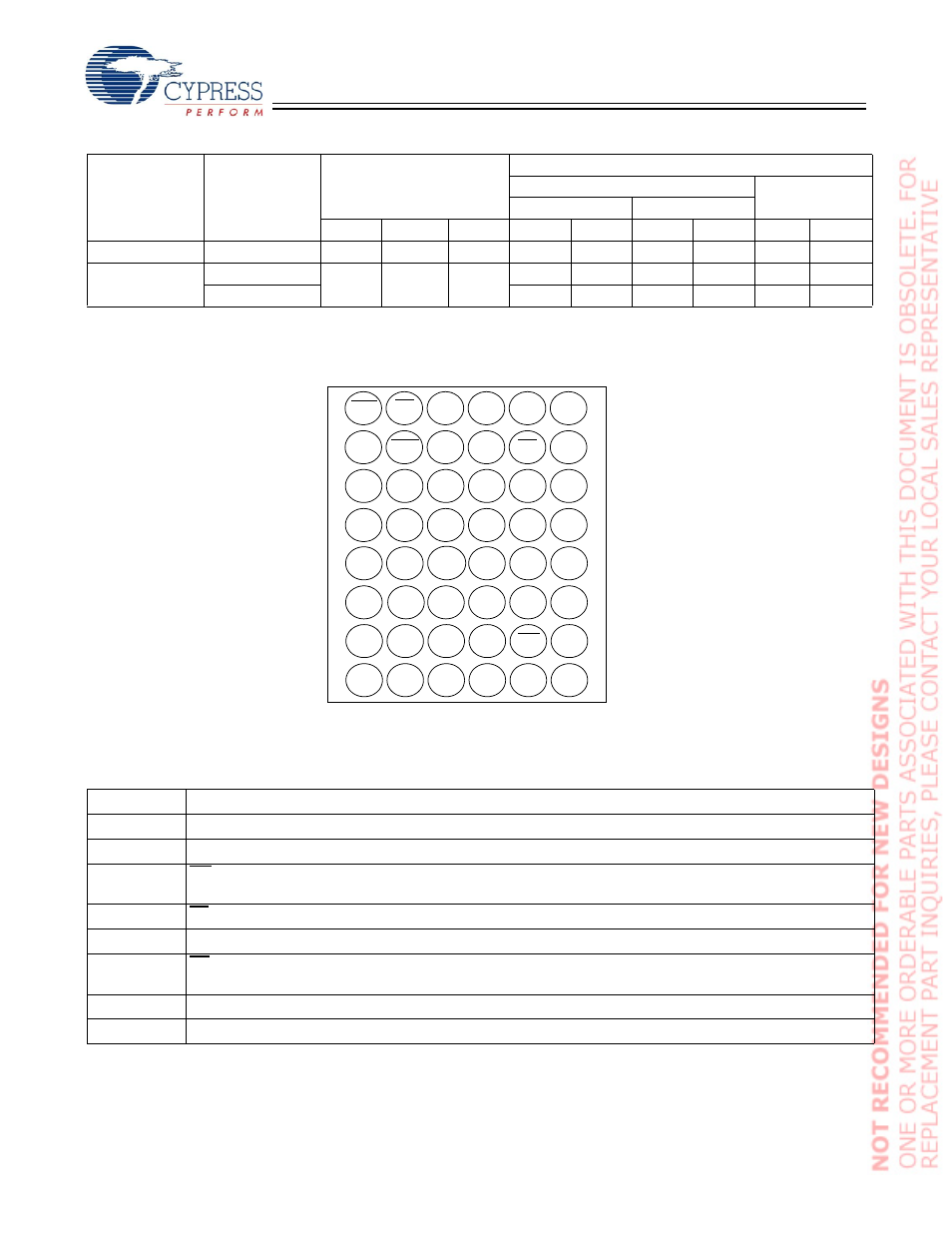
Pin Configurations
[2, 3, 4]
FBGA (Top View)
Pin Definitions
Name
Definition
Input
A
0
-A
18
. Address Inputs
Input/Output
I/O
0
-I/O
15
. Data lines. Used as input or output lines depending on operation
Input/Control
WE. Write Enable, Active LOW. When selected LOW, a WRITE is conducted. When selected HIGH, a READ is
conducted.
Input/Control
CE
1
. Chip Enable 1, Active LOW.
Input/Control
CE
2
. Chip Enable 2, Active HIGH.
Input/Control
OE. Output Enable, Active LOW. Controls the direction of the I/O pins. When LOW, the I/O pins behave as
outputs. When deasserted HIGH, I/O pins are three-stated, and act as input data pins
Ground
Vss. Ground for the device
Power Supply Vcc. Power supply for the device
Notes:
2. Typical values are included for reference only and are not guaranteed or tested. Typical values are measured at V
CC
= V
CC(typ.)
, T
A
= 25°C.
3. NC pins are not connected on the die.
4. E3 (DNU) can be left as NC or V
SS
to ensure proper application.
WE
A
11
A
10
A
6
A
0
A
3
CE
1
I/O
10
I/O
8
I/O
9
A
4
A
5
I/O
11
I/O
13
I/O
12
I/O
14
I/O
15
V
SS
A
9
A
8
OE
A
7
I/O
0
BHE
CE
2
A
17
A
2
A
1
BLE
V
CC
I/O
2
I/O
1
I/O
3
I/O
4
I/O
5
I/O
6
I/O
7
A
15
A
14
A
13
A
12
NC
A
18
NC
D
E
B
A
C
F
G
H
A
16
DNU
V
SS
V
CC
3
2
6
5
4
1