Jtag support – Cypress HOTLink II CYV15G0104TRB User Manual
Page 15
CYV15G0104TRB
Document #: 38-02100 Rev. *B
Page 15 of 27
Device Configuration Strategy
The following is a series of ordered events needed to load the
configuration latches on a per channel basis:
1. Pulse RESET Low after device power-up. This operation
resets both channels.
2. Set the static latch banks for the target channel.
3. Set the dynamic bank of latches for the target channel.
Enable the Receive PLL and/or transmit channel. If the
receiver is enabled, set the device for SMPTE data
reception (RXBISTA[1:0] = 01) or BIST data reception
(RXBISTA[1:0] = 10).
4. Reset the Phase Alignment Buffer. [Optional if phase align
buffer is bypassed.]
JTAG Support
The CYV15G0104TRB contains a JTAG port to allow system
level diagnosis of device interconnect. Of the available JTAG
modes, boundary scan, and bypass are supported. This
capability is present only on the LVTTL inputs and outputs, the
TRGCLKA± input, and the REFCLKB± clock input. The high-
speed serial inputs and outputs are not part of the JTAG test
chain.
3-Level Select Inputs
Each 3-Level select inputs reports as two bits in the scan
register. These bits report the LOW, MID, and HIGH state of
the associated input as 00, 10, and 11 respectively
JTAG ID
The JTAG device ID for the CYV15G0104TRB is ‘0C811069’x.
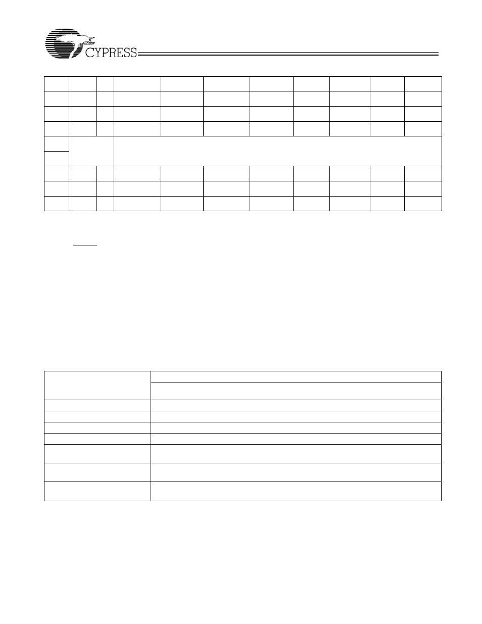
Table 5. Device Control Latch Configuration Table
ADDR
Channel
Type
DATA6
DATA5
DATA4
DATA3
DATA2
DATA1
DATA0
Reset
Value
0
(000b)
A
S
1
0
X
X
0
0
RXRATEA
1011111
1
(001b)
A
S
SDASEL2A[1]
SDASEL2A[0]
SDASEL1A[1]
SDASEL1A[0]
X
X
TRGRATEA
1010110
2
(010b)
A
D
RXBISTA[1]
RXPLLPDA
RXBISTA[0]
X
ROE2A
ROE1A
X
1011001
3
(011b)
INTERNAL TEST REGISTERS
DO NOT WRITE TO THESE ADDRESSES
4
(100b)
5
(101b)
B
S
X
X
X
X
X
0
X
1011111
6
(110b)
B
S
X
X
X
X
0
TXCKSELB
TXRATEB
1010110
7
(111b)
B
D
X
0
X
TXBISTB
TOE2B
TOE1B
PABRSTB
1011001
Table 6. Receive BIST Status Bits
{BISTSTA, RXDA[0], RXDA[1]}
Description
Receive BIST Status
(Receive BIST = Enabled)
000, 001
BIST Data Compare. Character compared correctly.
010
BIST Last Good. Last Character of BIST sequence detected and valid.
011
Reserved.
100
BIST Last Bad. Last Character of BIST sequence detected invalid.
101
BIST Start. Receive BIST is enabled on this channel, but character compares have not yet
commenced. This also indicates a PLL Out of Lock condition.
110
BIST Error. While comparing characters, a mismatch was found in one or more of the
character bits.
111
BIST Wait. The receiver is comparing characters but has not yet found the start of BIST
character to enable the LFSR.