Cypress CY14B101K User Manual
Features, Functional description, Logic block diagram
CY14B101K
1 Mbit (128K x 8) nvSRAM With Real Time Clock
Cypress Semiconductor Corporation
•
198 Champion Court
•
San Jose
,
CA 95134-1709
•
408-943-2600
Document Number: 001-06401 Rev. *I
Revised February 24, 2009
Features
■
25 ns, 35 ns, and 45 ns access times
■
Pin compatible with STK17TA8
■
Data integrity of Cypress nvSRAM combined with full featured
Real Time Clock (RTC)
❐
Low power, 350 nA RTC current
❐
Capacitor or battery backup for RTC
■
Watchdog timer
■
Clock alarm with programmable interrupts
■
Hands off automatic STORE on power down with only a small
capacitor
■
STORE to QuantumTrap™ initiated by software, device pin, or
on power down
■
RECALL to SRAM initiated by software or on power up
■
Infinite READ, WRITE, and RECALL cycles
■
High reliability
❐
Endurance to 200K cycles
❐
Data retention: 20 years at 55
°C
■
Single 3V operation with tolerance of +20%, –10%
■
Commercial and industrial temperature
■
48-Pin SSOP package (ROHS compliant)
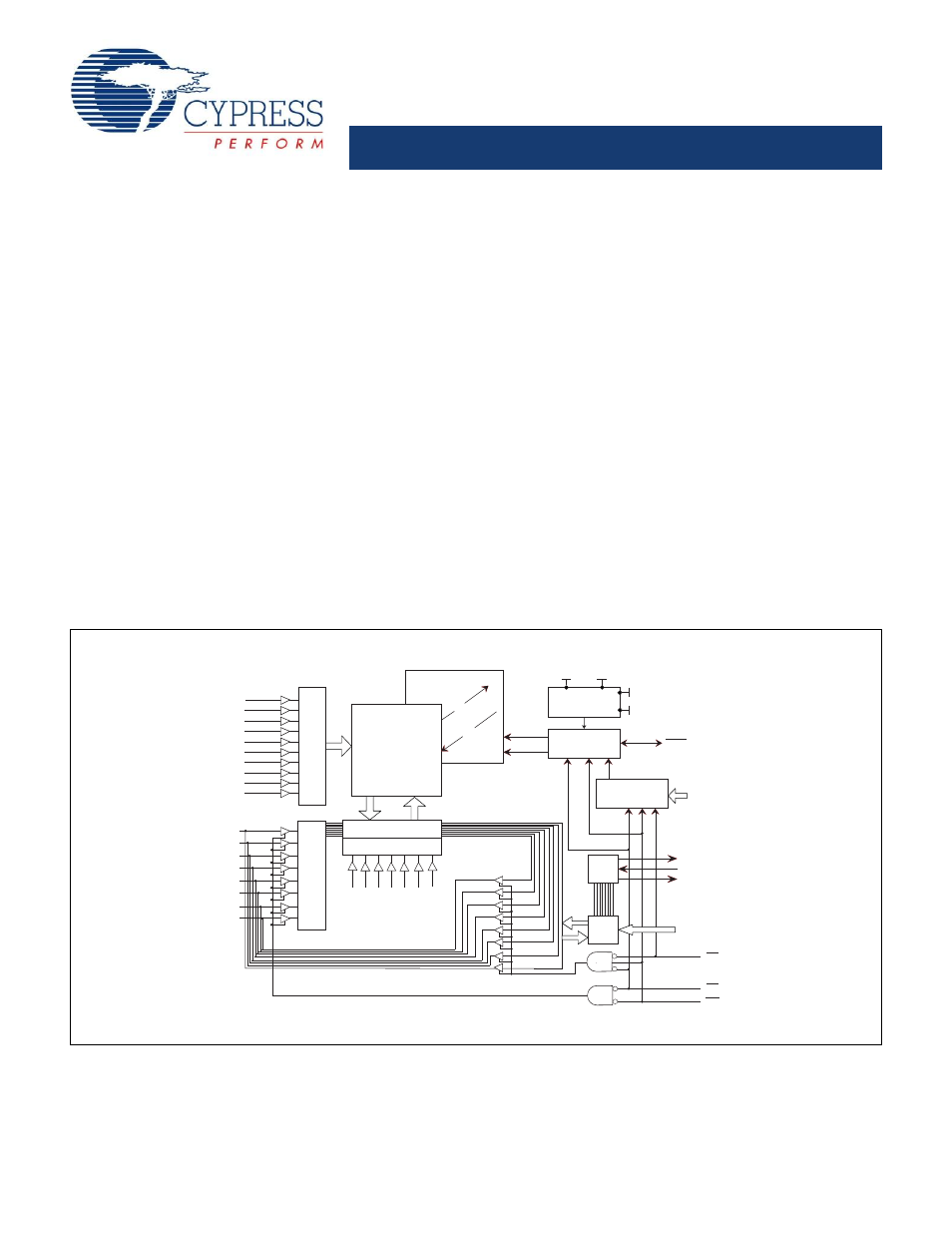
Functional Description
The Cypress CY14B101K combines a 1 Mbit nonvolatile static
RAM with a full featured real time clock in a monolithic integrated
circuit. The embedded nonvolatile elements incorporate
QuantumTrap technology producing the world’s most reliable
nonvolatile memory. The SRAM is read and written an infinite
number of times, while independent, nonvolatile data resides in
the nonvolatile elements.
The Real Time Clock function provides an accurate clock with
leap year tracking and a programmable high accuracy oscillator.
The alarm function is programmable for one time alarm or
periodic seconds, minutes, hours, or days. There is also a
programmable watchdog timer for process control.
STORE/
RECALL
CONTROL
POWER
CONTROL
SOFTWARE
DETECT
STATIC RAM
ARRAY
1024 X 1024
QuantumTrap
1024 x 1024
STORE
RECALL
COLUMN IO
COLUMN DEC
ROW DECODER
INPUT
BUFFERS
OE
CE
WE
HSB
V
CC
V
CAP
A
15
-
A
0
A
0
A
1
A
2
A
3
A
4
A
10
A
11
A
5
A
6
A
7
A
8
A
9
A
12
A
13
A
14
A
15
A
16
DQ
0
DQ
1
DQ
2
DQ
3
DQ
4
DQ
5
DQ
6
DQ
7
RTC
MUX
A
16
-
A
0
x
1
x
2
INT
V
RTCbat
V
RTCcap
Logic Block Diagram
Document Outline
- Features
- Functional Description
- Logic Block Diagram
- Pin Configurations
- Device Operation
- Real Time Clock Operation
- nvTIME Operation
- Clock Operations
- Reading the Clock
- Setting the Clock
- Backup Power
- Stopping and Starting the Oscillator
- Calibrating the Clock
- Alarm
- Watchdog Timer
- Power Monitor
- Interrupts
- Interrupt Register
- When an enabled interrupt source activates the INT pin, an external host reads the Flags registers to determine the cause. Remem...
- Flags Register
- Maximum Ratings
- Operating Range
- DC Electrical Characteristics
- Data Retention and Endurance
- Capacitance
- Thermal Resistance
- AC Test Conditions
- AC Switching Characteristics
- AC Switching Characteristics (continued)
- AutoStore or Power Up RECALL
- Software Controlled STORE/RECALL Cycles [21, 22]
- Hardware STORE Cycle
- Soft Sequence Commands
- RTC Characteristics
- Truth Table For SRAM Operations
- Part Numbering Nomenclature
- Ordering Information
- Package Diagrams
- Document History Page
- Sales, Solutions, and Legal Information