Cypress CYV15G0404DXB User Manual
Features, Functional description

CYV15G0404DXB
Independent Clock Quad HOTLink II™
Transceiver with Reclocker
Cypress Semiconductor Corporation
•
198 Champion Court
•
San Jose
,
CA 95134-1709
•
408-943-2600
Document #: 38-02097 Rev. *B
Revised December 14, 2007
Features
■
Quad channel transceiver for 195 to 1500 MBaud serial
signaling rate
❐
Aggregate throughput of up to 12 Gbits/second
■
Second-generation HOTLink
®
technology
■
Compliant to multiple standards
❐
SMPTE-292M, SMPTE-259M, DVB-ASI, Fibre Channel, ES-
CON, and Gigabit Ethernet (IEEE802.3z)
❐
10 bit uncoded data or 8B/10B coded data
■
Truly independent channels
❐
Each channel is able to:
• Perform reclocker function
• Operate at a different signaling rate
• Transport a different data format
■
Internal phase-locked loops (PLLs) with no external PLL
components
■
Selectable differential PECL compatible serial inputs per
channel
❐
Internal DC restoration
■
Redundant differential PECL compatible serial outputs per
channel
❐
No external bias resistors required
❐
Signaling rate controlled edge rates
❐
Source matched for 50
Ω transmission lines
■
MultiFrame™ Receive Framer provides alignment options
❐
Comma or full K28.5 detect
❐
Single or multibyte Framer for byte alignment
❐
Low latency option
■
Selectable input and output clocking options
■
Synchronous LVTTL parallel interface
■
JTAG boundary scan
■
Built In Self Test (BIST) for at-speed link testing
■
Link quality indicator by channel
❐
Analog signal detect
❐
Digital signal detect
■
Low power 3W at 3.3V typical
■
Single 3.3V supply
■
256 ball thermally enhanced BGA
■
0.25
μ BiCMOS technology
■
JTAG device ID ‘0C811069’x
Functional Description
The CYV15G0404DXB Independent Clock Quad HOTLink II™
Transceiver is a point-to-point or point-to-multipoint communica-
tions building block enabling the transfer of data over a variety of
high speed serial links including SMPTE 292, SMPTE 259, and
DVB-ASI video applications. The signaling rate can be anywhere
in the range of 195 to 1500 MBaud for each serial link. Each
channel operates independently with its own reference clock
allowing different rates. Each transmit channel accepts parallel
characters in an input register, encodes each character for
transport, and then converts it to serial data. Each receive
channel accepts serial data and converts it to parallel data,
decodes the data into characters, and presents these characters
to an output register. The received serial data can also be
reclocked and retransmitted through the serial outputs.
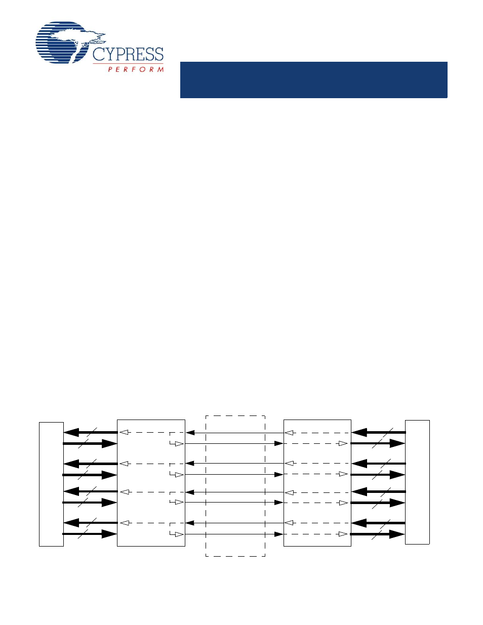
illustrates typical connections between independent video
coprocessors and corresponding CYV15G0404DXB chips.
Figure 1. HOTLink II™ System Connections
V
ideo Copro
ce
ssor
Serial Links
10
10
10
10
10
10
10
10
V
ideo
Cop
rocessor
10
10
10
10
10
10
10
10
Serial Links
Serial Links
Serial Links
Cable
Connections
Independent
CYV15G0404DXB
Independent
Reclocker
Reclocker
Channel
CYV15G0404DXB
Channel
Document Outline
- Features
- Functional Description
- CYV15G0404DXB Transceiver Logic Block Diagram
- Transmit Path Block Diagram
- Receive Path Block Diagram
- Device Configuration and Control Block Diagram
- Pin Configuration (Top View)
- Pin Configuration (Bottom View)
- Pin Definitions CYV15G0404DXB Quad HOTLink II Transceiver
- CYV15G0404DXB HOTLink II Operation
- Transmit BIST
- Serial Output Drivers
- CYV15G0404DXB Receive Data Path
- Output Bus
- Maximum Ratings
- Operating Range
- CYV15G0404DXB DC Electrical Characteristics
- AC Test Loads and Waveforms
- CYV15G0404DXB AC Electrical Characteristics
- CYV15G0404DXB Transmitter LVTTL Switching Characteristics Over the Operating Range
- CYV15G0404DXB Receiver LVTTL Switching Characteristics Over the Operating Range
- CYV15G0404DXB REFCLKx Switching Characteristics Over the Operating Range
- CYV15G0404DXB Bus Configuration Write Timing Characteristics Over the Operating Range
- CYV15G0404DXB JTAG Test Clock Characteristics Over the Operating Range
- CYV15G0404DXB Device RESET Characteristics Over the Operating Range
- CYV15G0404DXB Transmit Serial Outputs and TX PLL Characteristics Over the Operating Range
- CYV15G0404DXB Receive Serial Inputs and CDR PLL Characteristics Over the Operating Range
- Capacitance[20]
- CYV15G0404DXB HOTLink II Transmitter Switching Waveforms
- Switching Waveforms for the CYV15G0404DXB HOTLink II Receiver
- X3.230 Codes and Notation Conventions
- Ordering Information
- Package Diagram
