Cypress Rambus XDR CY24271 User Manual
Rambus, Xdr™ clock generator with zero sda hold time, Features

CY24272
Rambus
®
XDR™ Clock Generator with
Zero SDA Hold Time
Cypress Semiconductor Corporation
•
198 Champion Court
•
San Jose
,
CA 95134-1709
•
408-943-2600
Document Number: 001-42414 Rev. **
Revised November 9, 2007
Features
■
Meets Rambus
®
Extended Data Rate (XDR™) clocking
requirements
■
25 ps typical cycle-to-cycle jitter
❐
–135 dBc/Hz typical phase noise at 20 MHz offset
■
100 or 133 MHz differential clock input
■
300–667 MHz high speed clock support
■
Quad (open drain) differential output drivers
■
Supports frequency multipliers: 3, 4, 5, 6, 9/2 and 15/4
■
Spread Aware™
■
2.5V operation
■
28-pin TSSOP package
Table 1. Device Comparison
CY24271
CY24272
SDA hold time = 300 ns
(SMBus compliant)
SDA hold time = 0 ns
(I
2
C compliant)
R
RC
= 200
Ω typical
(Rambus standard drive)
R
RC
= 295
Ω minimum
(Reduced output drive)
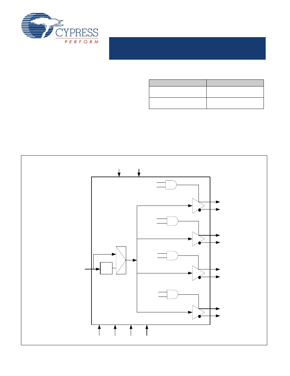
CLK0
CLK0B
CLK1
CLK1B
CLK2
CLK2B
CLK3
CLK3B
REFCLK,REFCLKB
SCL
SDA
ID0
ID1
EN
RegA
EN
RegB
EN
RegC
EN
RegD
PLL
Bypass
MUX
/BYPASS
EN
Logic Block Diagram
Document Outline
- Features
- Logic Block Diagram
- Input Clock Signal
- Modes of Operation
- Device ID and SMBus Device Address
- SMBus Protocol
- SMBus Data Byte Definitions
- Absolute Maximum Conditions
- DC Operating Conditions
- AC Operating Conditions
- DC Electrical Specifications
- AC Electrical Specification
- Test and Measurement Setup
- Example External Resistor Values and Termination Voltages for a 50W Channel
- Signal Waveforms
- Jitter
- Ordering Information
- Package Drawing and Dimension
- Document History Page
