Switching characteristics, Switching waveforms – Cypress 256K (32K x 8) CY62256 User Manual
Page 4
CY62256
Document #: 38-05248 Rev. *B
Page 4 of 11
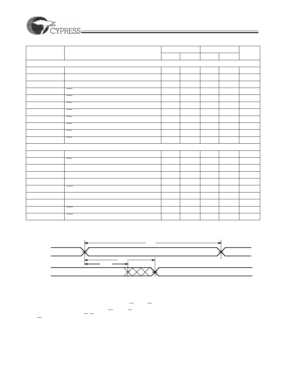
Switching Characteristics
Over the Operating Range
[6]
Parameter
Description
CY62256
−
55
CY62256
−
70
Unit
Min.
Max.
Min.
Max.
Read Cycle
t
RC
Read Cycle Time
55
70
ns
t
AA
Address to Data Valid
55
70
ns
t
OHA
Data Hold from Address Change
5
5
ns
t
ACE
CE LOW to Data Valid
55
70
ns
t
DOE
OE LOW to Data Valid
25
35
ns
t
LZOE
OE LOW to Low-Z
[7]
5
5
ns
t
HZOE
OE HIGH to High-Z
[7, 8]
20
25
ns
t
LZCE
CE LOW to Low-Z
[7]
5
5
ns
t
HZCE
CE HIGH to High-Z
[7, 8]
20
25
ns
t
PU
CE LOW to Power-up
0
0
ns
t
PD
CE HIGH to Power-down
55
70
ns
Write Cycle
[9, 10]
t
WC
Write Cycle Time
55
70
ns
t
SCE
CE LOW to Write End
45
60
ns
t
AW
Address Set-up to Write End
45
60
ns
t
HA
Address Hold from Write End
0
0
ns
t
SA
Address Set-up to Write Start
0
0
ns
t
PWE
WE Pulse Width
40
50
ns
t
SD
Data Set-up to Write End
25
30
ns
t
HD
Data Hold from Write End
0
0
ns
t
HZWE
WE LOW to High-Z
[7, 8]
20
25
ns
t
LZWE
WE HIGH to Low-Z
[7]
5
5
ns
Switching Waveforms
Notes:
6.
Test conditions assume signal transition time of 5 ns or less, timing reference levels of 1.5V, input pulse levels of 0 to 3.0V, and output loading of the specified
I
OL
/I
OH
and 100-pF load capacitance.
7.
At any given temperature and voltage condition, t
HZCE
is less than t
LZCE
, t
HZOE
is less than t
LZOE
, and t
HZWE
is less than t
LZWE
for any given device.
8.
t
HZOE
, t
HZCE
, and t
HZWE
are specified with C
L
= 5 pF as in (b) of AC Test Loads. Transition is measured
±
500 mV from steady-state voltage.
9.
The internal Write time of the memory is defined by the overlap of CE LOW and WE LOW. Both signals must be LOW to initiate a Write and either signal can terminate
a Write by going HIGH. The data input set-up and hold timing should be referenced to the rising edge of the signal that terminates the Write.
10. The minimum Write cycle time for Write cycle #3 (WE controlled, OE LOW) is the sum of t
HZWE
and t
SD
11. Device is continuously selected. OE, CE = V
IL
.
12. WE is HIGH for Read cycle.
ADDRESS
DATA OUT
PREVIOUS DATA VALID
DATA VALID
t
RC
t
AA
t
OHA
Read Cycle No. 1
[11, 12]