Pin configurations, Pin definitions, Stk11c68 – Cypress STK11C68 User Manual
Page 2

STK11C68
Document Number: 001-50638 Rev. **
Page 2 of 16
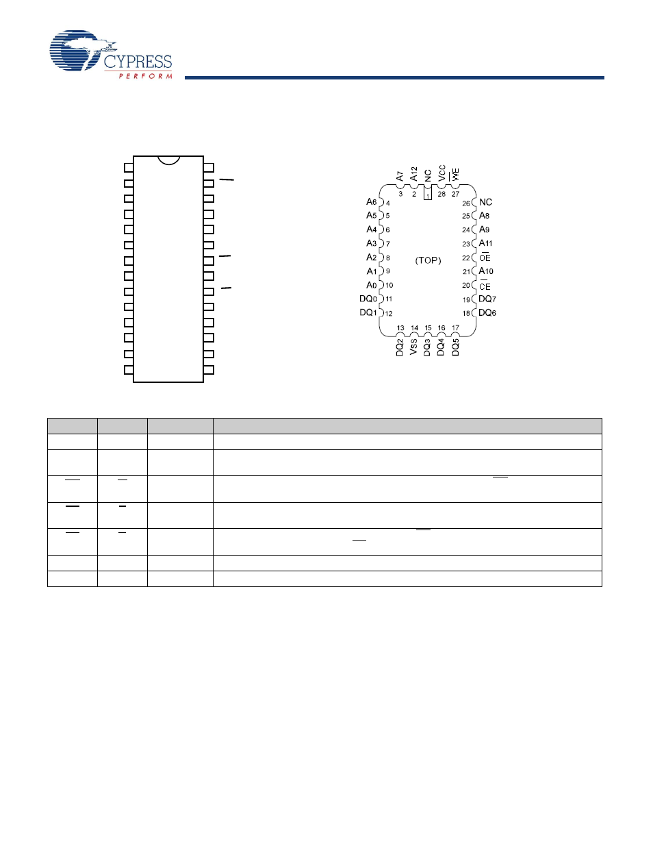
Pin Configurations
Figure 1. Pin Diagram - 28-Pin SOIC/DIP and 28-Pin LLC
Pin Definitions
Pin Name
Alt
IO Type
Description
A
0
–A
12
Input
Address Inputs. Used to select one of the 8,192 bytes of the nvSRAM.
DQ
0
-DQ
7
Input or
Output
Bidirectional Data IO Lines. Used as input or output lines depending on operation.
WE
W
Input
Write Enable Input, Active LOW. When the chip is enabled and WE is LOW, data on the
IO pins is written to the specific address location.
CE
E
Input
Chip Enable Input, Active LOW. When LOW, selects the chip. When HIGH, deselects the
chip.
OE
G
Input
Output Enable, Active LOW. The active LOW OE input enables the data output buffers
during read cycles. Deasserting OE HIGH causes the IO pins to tri-state.
V
SS
Ground
Ground for the Device. The device is connected to ground of the system.
V
CC
Power Supply Power Supply Inputs to the Device.
1&
$
$
$
$
$
$
$
$
'4
'4
'4
9
66
9
&&
1&
$
$
$
$
'4
'4
'4
'4
'4
$
:(
2(
&(
723
- CY7C1410AV18 (29 pages)
- CY7C1411JV18 (28 pages)
- CY7C1383FV25 (28 pages)
- CY14B256L (18 pages)
- CY7C1307BV25 (21 pages)
- CY7C1041DV33 (13 pages)
- CY62167EV18 (13 pages)
- Perform CY7C1565V18 (28 pages)
- STK11C68-5 (15 pages)
- 7C185-20 (11 pages)
- CY7C1168V18 (27 pages)
- CY7C1318CV18-250BZC (26 pages)
- CY7C1364C (18 pages)
- Perform CY7C1382D (34 pages)
- CY7C106D (11 pages)
- CY14E102N (21 pages)
- CY7C1418AV18 (31 pages)
- enCoRe CY7C638xx (83 pages)
- CY7C1018DV33 (9 pages)
- CY7C1292DV18 (23 pages)
- CY7C130 (19 pages)
- CY7C1424BV18 (30 pages)
- CY62157EV18 (12 pages)
- CY7C1392BV18 (31 pages)
- CY7C1302DV25 (18 pages)
- Perform CY7C1511KV18 (31 pages)
- West Bridge Astoria AN46860 (4 pages)
- CY7C1386FV25 (30 pages)
- CY7C1163V18 (29 pages)
- CY7C1266V18 (27 pages)
- CY7C1334H (13 pages)
- CY7C1018CV33 (7 pages)
- CY62136VN (12 pages)
- AN20639 (3 pages)
- CY7C1338G (17 pages)
- CY7C1462AV33 (27 pages)
- CY7C1145V18 (28 pages)
- STK11C88 (15 pages)
- CY7C1231H (12 pages)
- Perform CY7C142 (15 pages)
- CY14E256L (18 pages)
- STK15C88 (15 pages)
- CY7C1297H (15 pages)
- CY7C1441AV33 (31 pages)
- CapSense CY8C20x36 (34 pages)
