Method 2 - regulated power supply connection at j1 – Welch Allyn Poem NIBP Module DeveloperS Kit Instructions - Installation Guide User Manual
Page 4
POEM NIBP Module Developer’s Kit Instructions
Welch Allyn OEM Technologies
Page 4
Confidential
810-1209-01 Rev. A
The basic requirement at J2 is a supply that never drops below 6.0 Vdc at maximum load, never
rises above 15 Vdc when unloaded, and can deliver at least 6 W while meeting these voltage
requirements. Note that between NIBP readings, the POEM Module enters a low power sleep
mode which allows the power adapter output to rise almost to its unloaded voltage (unloaded
voltage of non-regulated power adapters will likely be 25% to 50% higher than voltage at rated
current, so check any adapter not supplied by Welch Allyn OEM Technologies).
If an unregulated adapter’s unloaded voltage is high enough to turn on Transzorb D6 in the
POEM Module, but not high enough to blow Fuse F1 on the Interface Board, the POEM Module
may be damaged. Also, while reprogramming the Module, higher voltage at J2 increases heating
in the Interface Board’s 5 V regulator. Based on these factors, an unregulated or regulated power
adapter rated at greater than or equal to 6 W at 6 to 9 Vdc is recommended. When given this
input, the Module and Interface Board fulfill all other power requirements.
NOTE
If the wrong polarity is applied to J2, the Module and Interface Board are not powered
and no damage occurs.
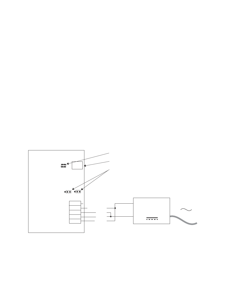
METHOD 2 - Regulated Power Supply Connection at J1
The simplest regulated power supply configuration requirements are shown in Figure 3. Refer to
the
POEM NIBP Module OEM Implementation Manual
for details about more complex power
supply configurations.
Figure 3 - Regulated Power Supply Configuration
CAUTION
Incorrect polarity at J1 will damage the power supply, the Interface Board,
and/or the POEM Module. Refer to the POEM OEM Implementation Manual for
more information.
JMPR2 JMPR1
1
1
1 2
P1
3 4
J1
J2
REGULATED DC
POWER SUPPLY
4.75 to 5.25 V
≥ 1 A
AC Input
P1 configuration does not matter.
Leave J2 unconnected.
Configure JMPR1 and JMPR2 as shown.
HOST_3.3V
HOST_5V
GND
GND
VBUS
+
_
VBUS = +4.75 to +15.5 V (consumption ~3 W peak, worst case)
HOST_5V = +4.75 to +5.25 V (consumption up to 75 mA, worst case)
HOST_3.3V (optional) = +3.1 to +3.4 V (consumption up to 65 mA,
worst case)