Chapter 4 programming pb-tim2 user’s manual – Kontron PB-TIM2 User Manual
Page 28
Chapter 4 Programming
PB-TIM2 User’s Manual
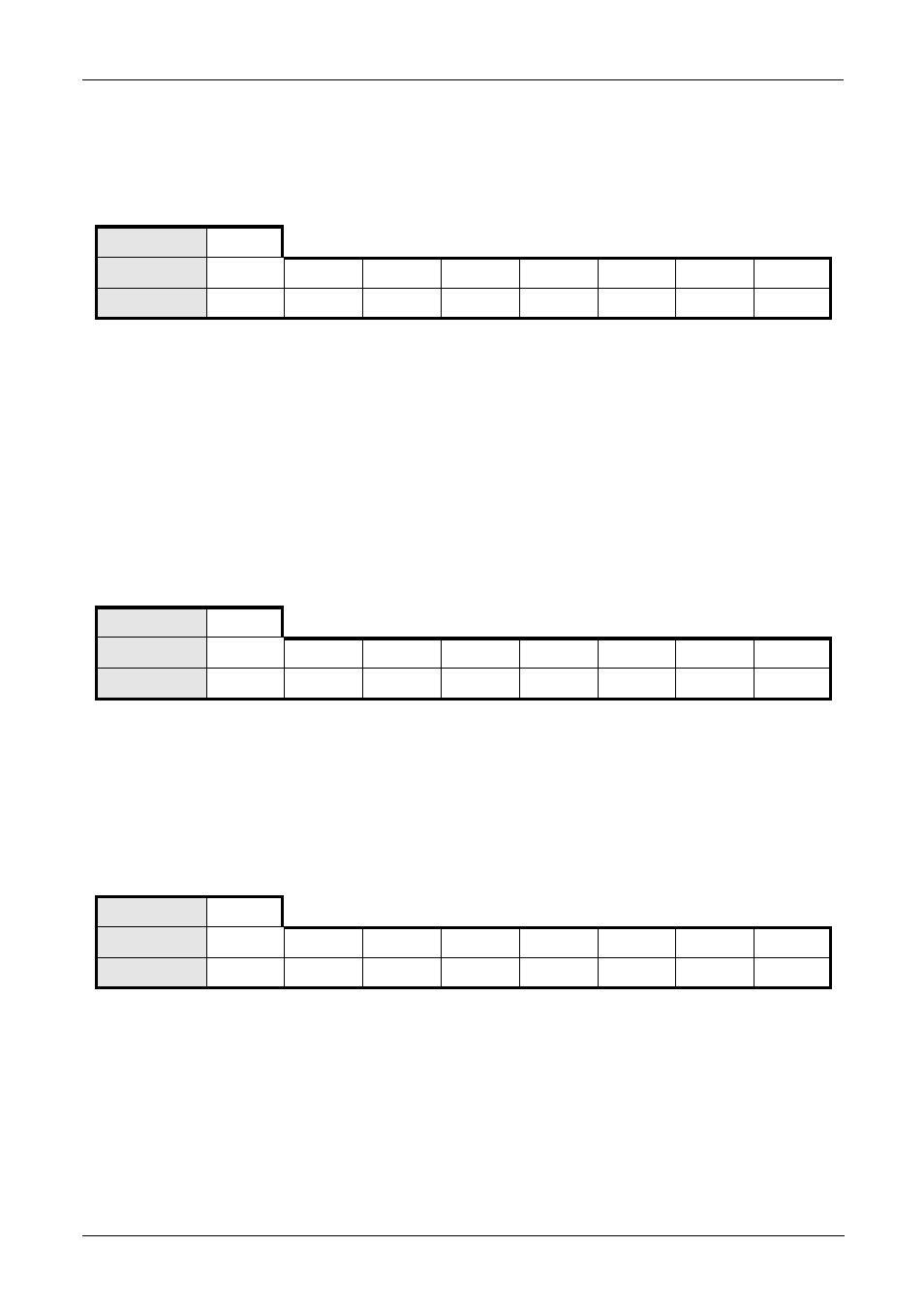
4.2.13 Write EEPROM Access Register
Write Only Register
Address
$7E
Bit
b7
b6
b5
b4
b3
CLK
CS
WDATA
After Reset
0
0
0
Where •
WDATA :
This contains the bit that has to be written to the EEPROM
• CS :
The status of the EEPROM chip select (0 = disabled, 1 = enabled)
• CLK :
Value of the SPI clock pin to access the EEPROM
Data is written to the EEPROM at one bit at a time and only then when the EEPROM is chip selected. This serial bit
transfer is clocked with the SPI clock.
4.2.14 Read EEPROM Access Register
Read Only Register
Address
$7E
Bit
b7
b6
b5
b4
b3
CLK
CS
RDATA
After Reset
x
x
x
x
x
x
x
0
Where •
RDATA :
This shows the current value of the SPIDI (SPI data input)
4.2.15 Software ID Byte
Read Only Register
Address
$79
Bit
b7
b6
b5
b4
b3
b2
b1
b0
After Reset
0
0
0
0
0
0
0
1
The value is $01 and allows identification of the FPGA program version. Changes in the FPGA program will be
reflected in this ID byte such that the software can automatically adjust.
Page 4-8
© 1996 PEP Modular Computers
July 30, 1997