Pb-tim2 user’s manual chapter 4 programming – Kontron PB-TIM2 User Manual
Page 27
PB-TIM2 User’s Manual
Chapter 4 Programming
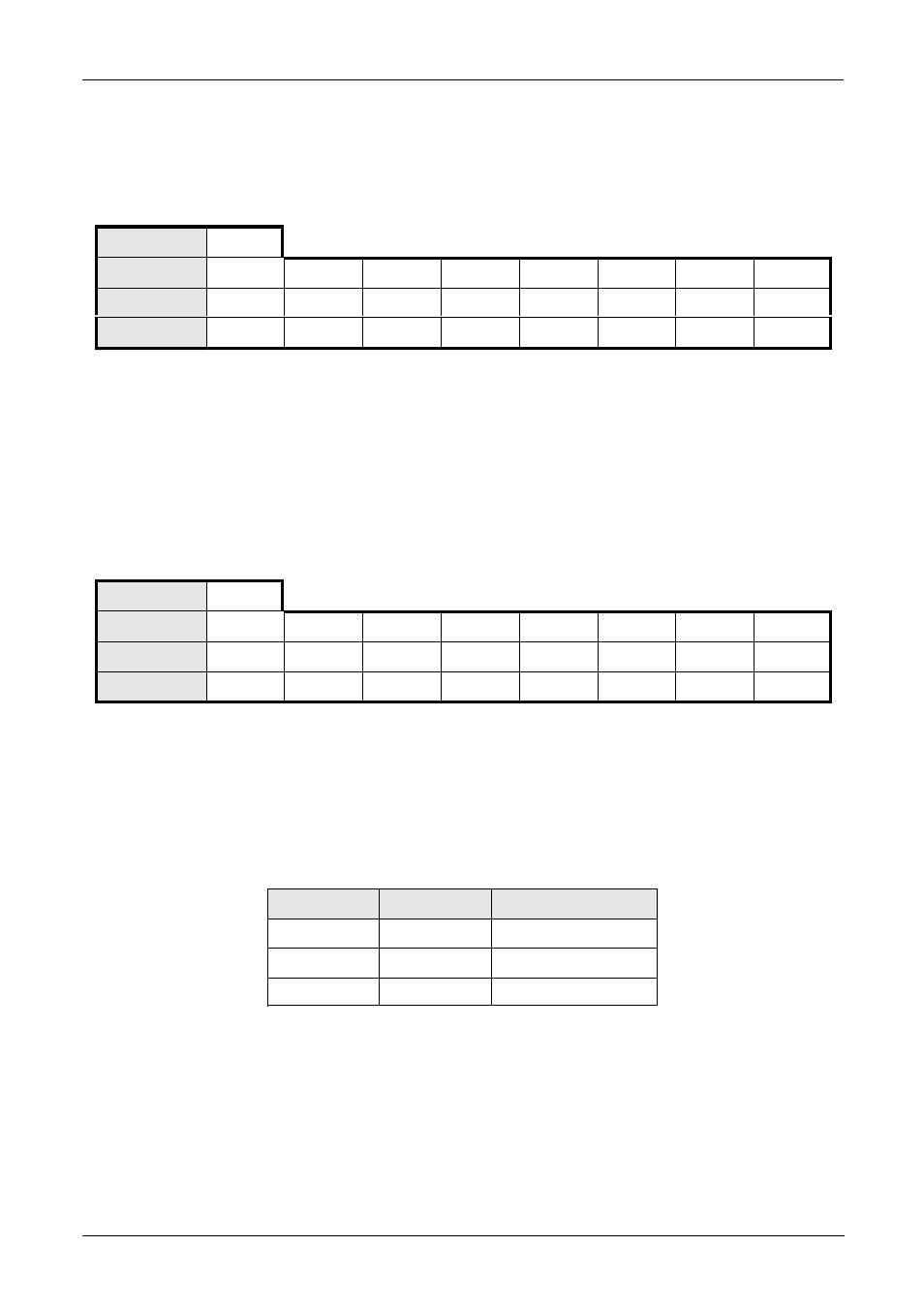
4.2.11 Common Interrupt Authorization Register
Write Only Register
Address
$69
Bit
7
6
5
4
3
2
1
0
Function
CH 2
CH 1
CH 0
After Reset
0
0
0
Where • CH x :
A 1 in this position authorizes interrupts from the corresponding timer
4.2.12 Interrupt Vector
Write Only Register
Address
$6D
Bit
7
6
5
4
3
2
1
0
Function
V7
V6
V5
V4
V3
V2
IS1
IS0
After Reset
0
0
0
0
0
0
x
x
Where •
V2-V7 :
Programmable interrupt vector bits
Upon receipt of an INTACK signal, the interrupt vector register is placed on the data bus
• IS0 & IS1 :
Shows the interrupt source as in the following table
I S 1
I S 0
Interrupt Source
0
1
Channel 0
1
0
Channel 1
1
1
Channel 2
If an interrupt is generated, a vector is placed on the data bus during the INTACK signal. The upper 6 bits of this vector
are user definable while the two lower bits define the interrupt source. Pending interrupts are latched in a corresponding
register and an interrupt may be cleared by writing a bit in the Interrupt Clear Register. In the event that several
interrupts have been generated, the signals will remain active until all have been serviced.
Note : All interrupt sources are edge triggered.
July 30, 1997
© 1996 PEP Modular Computers
Page 4-7