Chapter 4 programming pb-tim2 user’s manual – Kontron PB-TIM2 User Manual
Page 26
Chapter 4 Programming
PB-TIM2 User’s Manual
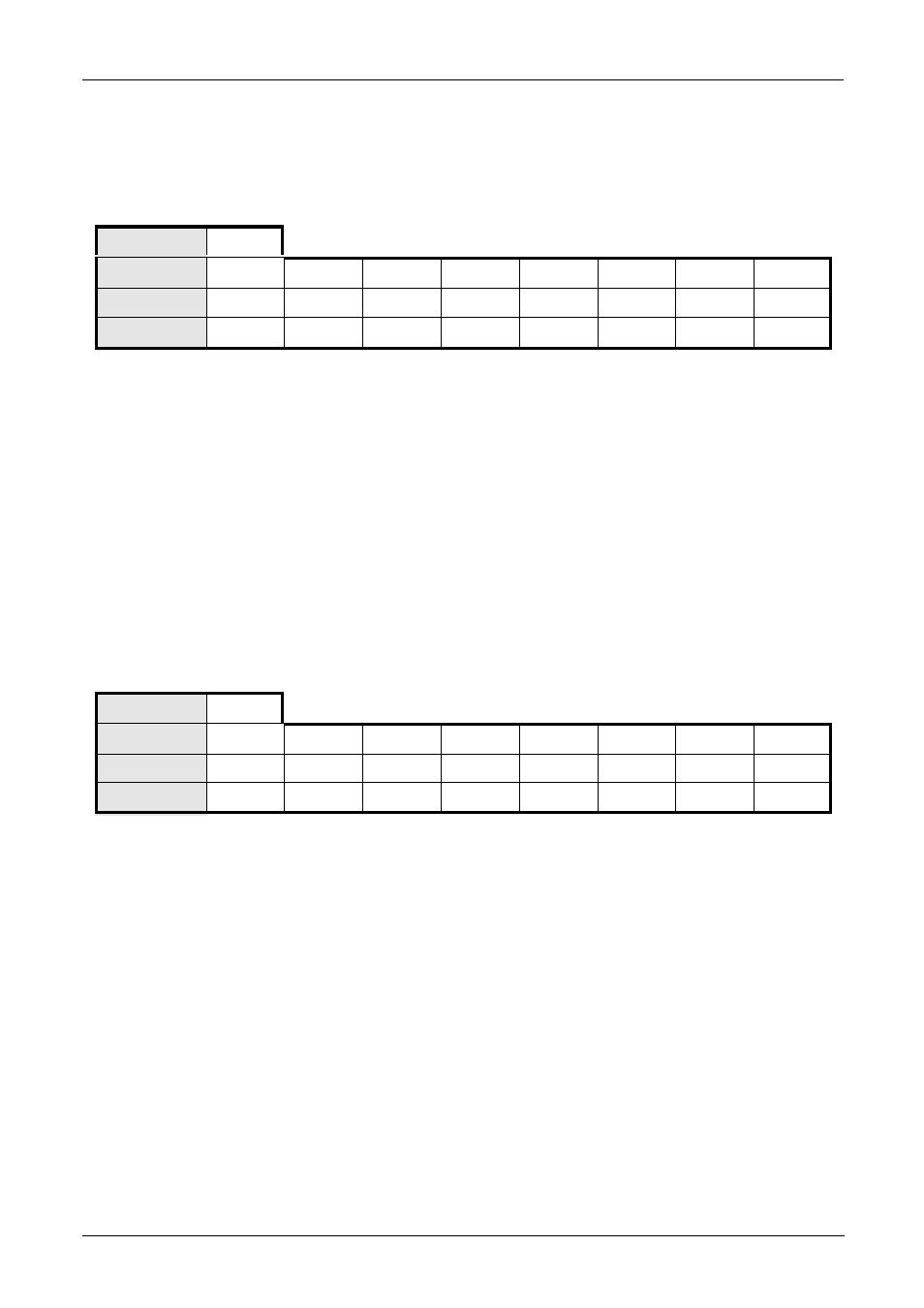
4.2.9 Common Control Register
Write Only Register
Address
$61
Bit
7
6
5
4
3
2
1
0
Function
PWM 1
T IN 2
ST2
ST1
ST0
After Reset
0
0
0
0
0
Where •
STx :
Authorizes common clear function on corresponding channel
• T IN 2 :
Defines the operation of timer channel 2. A 1 in this location will link the
output of channel 0 to the counter clock of channel 2 (channel 0 and 2 will
also be cascaded)
• PWM 1 :
Defines the operation of channel 1. A 1 in this location will internally link the
output of channel 0 to the (A) input of channel 1 and the output of channel 1 to the
(A) input of channel 0. With this configuration, both channels generate half
a Pulse
Width Modulation signal
4.2.10 Common Interrupt Pending Register
Read Only Register
Address
$65
Bit
7
6
5
4
3
2
1
0
Function
CH 2
CH 1
CH 0
After Reset
0
0
0
Where • CH x :
A 1 in this position means an interrupt pending from the corresponding channel
Note : If an interrupt is pending from a given channel then the only way to clear it is to use the channel interrupt clear
register.
Page 4-6
© 1996 PEP Modular Computers
July 30, 1997