An364 – Cirrus Logic AN364 User Manual
Page 9
AN364
AN364REV3
9
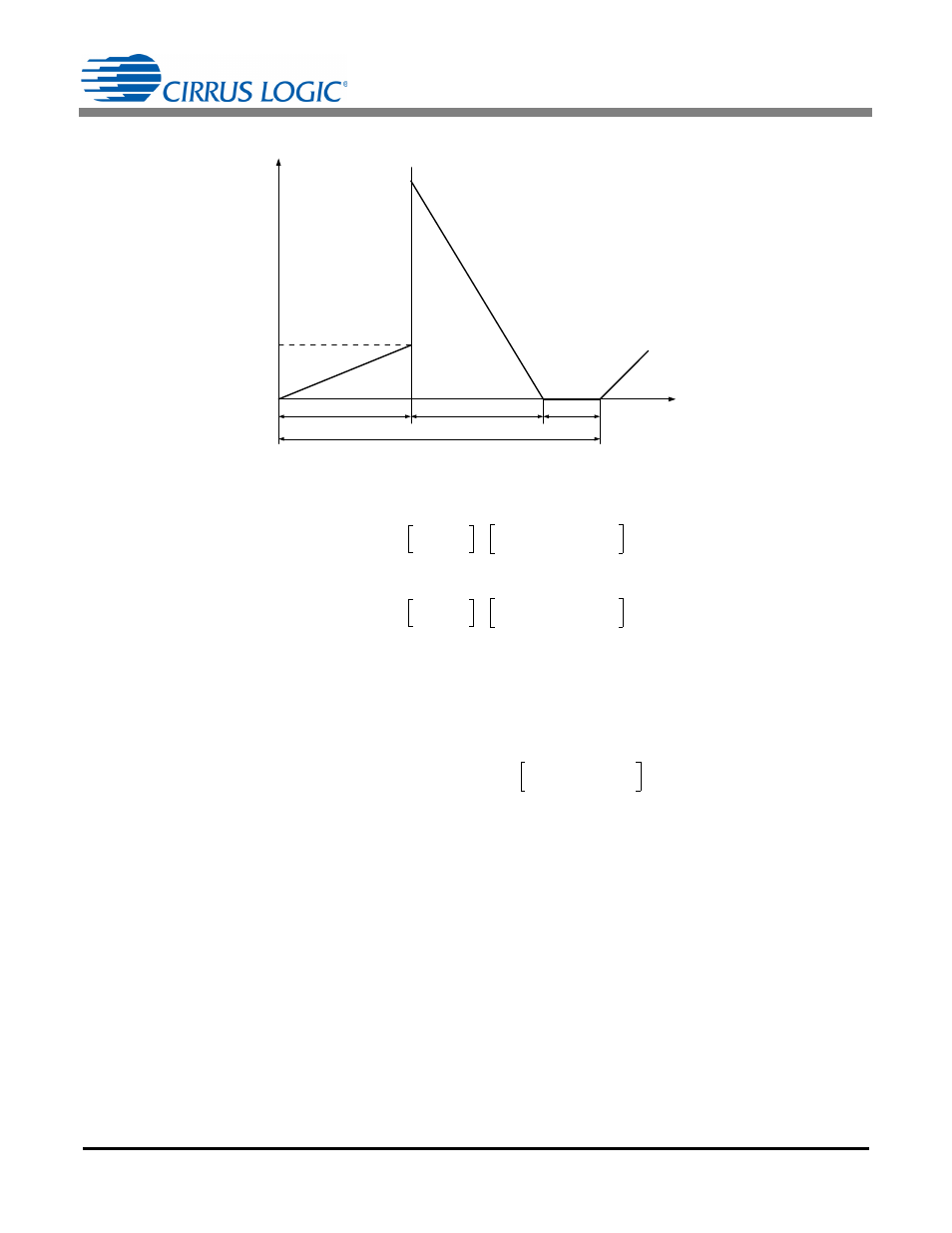
Figure 4 illustrates the switching frequency used in the system design.
Solve for T1 and T2 using Equation 7 and Equation 8:
Period T1 is limited to a maximum duration of 8.8
s by the IC algorithm. Verify that period T1 at full power is
less that 7.8
s, leaving sufficient time for a probe cycle, which requires a slightly longer T1 period.
Step 6) Calculate Peak Current on the Flyback Primary-side
Calculate I
PK(FB)
using Equation 9:
where
TT
fb
= switching period at full brightness (full load condition)
T1
fb
= period T1 at full brightness (full load condition)
Step 7) Calculate R
Sense
(R23)
Calculate sense resistor R
Sense
(R23) for flyback using Equation 10:
where
R23 = R
Sense
in
Step 8) Calculate the Flyback Primary-side Inductance
t
i(t)
T1
T2
TT
No Current
T3
Peak Primary Current, I
PK(FB)
Primary
Current
Secondary
Current
Figure 4. Timing Diagram of T1, T2, T3, and TT
T1
1
F
sw
--------- T3
–
V
Reflected
V
Reflected
V
BST
+
----------------------------------------------------
=
[Eq. 7]
T2
1
F
sw
--------- T3
–
V
BST
V
Reflected
V
BST
+
----------------------------------------------------
=
[Eq. 8]
I
PK FB
2 P
OUT max
TT
fb
V
BST
T1
fb
----------------------------------------------
=
[Eq. 9]
R
Sense
1.4V
I
PK FB
------------------
=
[Eq. 10]
L
P
V
BST
T1
I
PK FB
---------------------------
=
[Eq. 11]