2 boost stage design steps, An364 – Cirrus Logic AN364 User Manual
Page 22
AN364
22
AN364REV3
calculate the transformer T1 secondary RMS current:
Step 11) Determine Output Capacitor
Output capacitor C5 ripple current I
Ripple(RMS)
is the vectorial difference between transformer T1 secondary
current and the DC load current. See Equation 39.
Output capacitor C5 is selected as a 100
F, 25V capacitor.
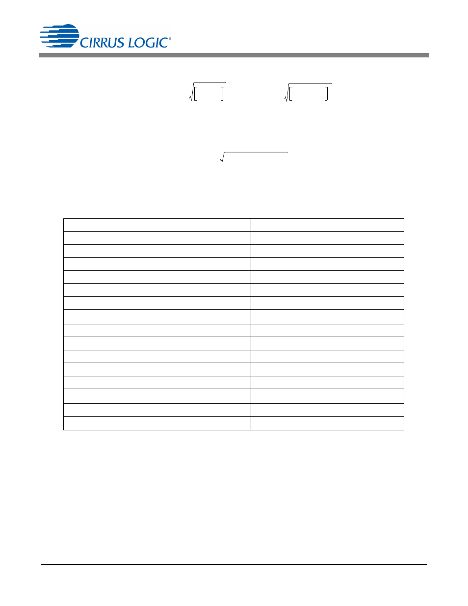
Step 12) Flyback Transformer Specification
Specifications for the flyback transformer T1 can now be compiled to enable suppliers to design within size
and cost constraints.
Step 13) Circuit Adjustments
Now that the transformer has been defined and built, it may need to be adjusted. For more information, see
Circuit Adjustments on page 11.
Validate that the system meets the operating criteria. This may require adjusting components like R
Sense
and
R
FBGAIN
. For more information, see Recalculate R
4.2 Boost Stage Design Steps
Using Equation 19, calculate I
PK(BST)
:
Parameter
Value
Output DC Power
6.6W
Converter Topology
CRM flyback
Switching Frequency
85kHz
Primary Inductance
11.3 mH
10%
Peak Primary Current
0.15A
Primary RMS Current
43mA
Turns Ratio N
P
/N
S
14.3
Secondary Voltage
15.4V
Secondary RMS Current
0.85A
Primary Leakage Inductance
<100
H
Primary Voltage
405V
Electrostatic Shield
Between primary and secondary winding
Auxiliary Winding Turns Ratio (N
P
/N
AUX
)
20
Auxiliary Wire
Any convenient gauge
Rigidity Sec
Core/Primary/Aux/Shield
>2,500V
I
RMS
I
PK FB
N
T
current
3 TT
--------------------
=
0.131A 14.3
7.45
s
3 12.5
s
----------------------------
850mA
=
=
[Eq. 38]
I
Ripple RMS
0.85A
2
0.44A
2
–
0.73A
=
=
[Eq. 39]
I
PK BST
3.64 P
IN
V
RMS
---------------------------
3.64 7.3W
230V
--------------------------------
116mA
=
=
=
[Eq. 40]