3 flyback stage design, An364 – Cirrus Logic AN364 User Manual
Page 6
AN364
6
AN364REV3
3.3 Flyback Stage Design
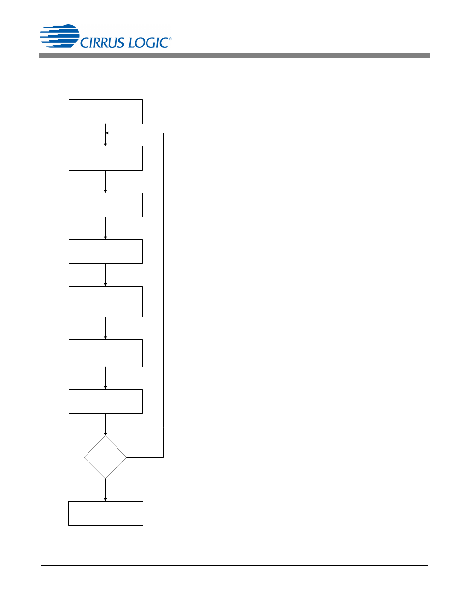
Figure 2 illustrates the steps for designing the flyback stage.
Figure 2. Flyback Stage Design
Flyback Specification
Determine N, F
sw
,
V
Reflected
, and V
CLAMP
Estimate T3
Calculate TT
fb
Calculate R
Sense
,
R
FBGAIN
, and Primary
Inductance
R
Sense
,R
FBGAIN
Fit?
Yes
No
Calculate T1,
T2, and I
PK(FB )
Calculate RMS Current
and Output Capacitor
Transformer Core
Steps for the Flyback Design
1. Set boost output voltage V
BST
.
2. Select a MOSFET that aligns with the quality standards of
the designer’s company.
3. Determine the transformer turns ratio from the
V
BST
, FET
voltage, and reflected voltage V
Reflected
.
4. Use the nominal switching frequency and an initial
estimate for time T3 to determine the value of time TT at
full brightness.
5. Use V
BST
, TT, and V
Reflected
to determine time T1 and T2.
6. Use time T2 and TT, turns ratio N and load current to
determine the value of peak primary current I
PK(FB)
.
7. Use I
PK(FB)
to determine R
Sense
.
8. Calculate the primary side inductance using time T1.
9. Calculate flyback gain resistor R
FBGAIN
using full load
conditions. Ensure linearity of the load versus the dim
curve.
10. Calculate primary and secondary RMS currents using
I
PK(FB)
and duty cycle.
11. Select an output capacitor.
12. Determine the flyback transformer specifications.
13. Determine if the flyback transformer fits into specified form
factor after designing and constructing flyback transformer.
Repeat steps 3 to 12 until form factor criteria is met.
14. Refine the circuit using the final flyback transformer
design.
15. Validate that the system meets the operating criteria.