Conversion data output descriptions – Cirrus Logic CS5534-AS User Manual
Page 37
CS5531/32/33/34-AS
DS289F5
37
2.8.1. Conversion Data Output Descriptions
CS5531/33 (16-BIT CONVERSIONS)
CS5532/34 (24-BIT CONVERSIONS)
Conversion Data Bits [31:16 for CS5531/33; 31:8 for CS5532/34]
These bits depict the latest output conversion.
NU (Not Used) [15:3 for CS5531/33; 7:3 for CS5532/34]
These bits are masked logic zero.
OF (Over-range Flag Bit) [2]
0
Bit is clear when over-range condition has not occurred.
1
Bit is set when input signal is more positive than the positive full scale, more negative than zero (unipolar
mode) or when the input is more negative than the negative full scale (bipolar mode).
CI (Channel Indicator Bits) [1:0]
These bits indicate which physical input channel was converted.
00
Physical Channel 1
01
Physical Channel 2
10
Physical Channel 3
11
Physical Channel 4
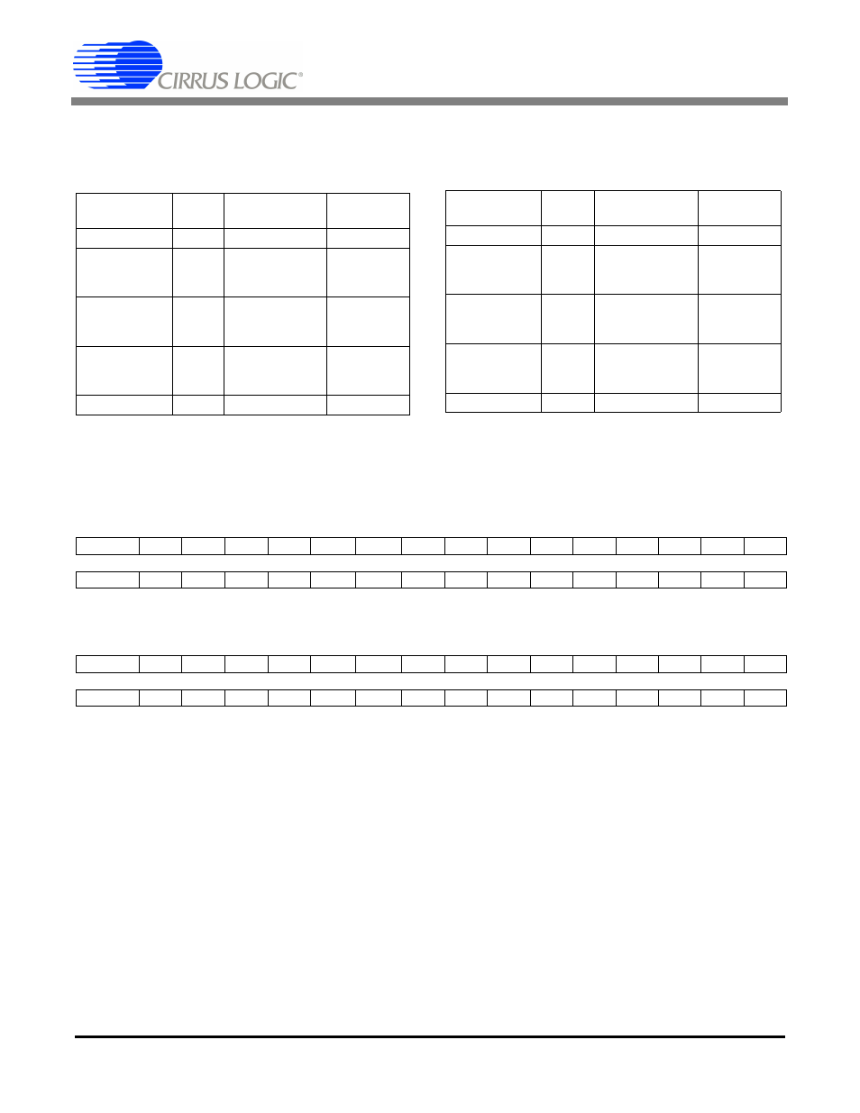
Table 4. Output Coding for 16-bit CS5531 and CS5533
Unipolar Input
Voltage
Offset
Binary
Bipolar Input
Voltage
Two's
Complement
>(VFS-1.5 LSB)
FFFF
>(VFS-1.5 LSB)
7FFF
VFS-1.5 LSB
FFFF
------
FFFE
VFS-1.5 LSB
7FFF
------
7FFE
VFS/2-0.5 LSB
8000
------
7FFF
-0.5 LSB
0000
------
FFFF
+0.5 LSB
0001
------
0000
-VFS+0.5 LSB
8001
------
8000
<(+0.5 LSB)
0000
<(-VFS+0.5 LSB)
8000
Table 5. Output Coding for 24-bit CS5532 and CS5534
Unipolar Input
Voltage
Offset
Binary
Bipolar Input
Voltage
Two's
Complement
>(VFS-1.5 LSB) FFFFFF >(VFS-1.5 LSB)
7FFFFF
VFS-1.5 LSB
FFFFFF
------
FFFFFE
VFS-1.5 LSB
7FFFFF
------
7FFFFE
VFS/2-0.5 LSB 800000
------
7FFFFF
-0.5 LSB
000000
------
FFFFFF
+0.5 LSB
000001
------
000000
-VFS+0.5 LSB
800001
------
800000
<(+0.5 LSB)
000000 <(-VFS+0.5 LSB)
800000
D31(MSB) D30
D29
D28
D27
D26
D25
D24
D23
D22
D21
D20
D19
D18
D17
D16
MSB
14
13
12
11
10
9
8
7
6
5
4
3
2
1
LSB
D15
D14
D13
D12
D11
D10
D9
D8
D7
D6
D5
D4
D3
D2
D1
D0
0
0
0
0
0
0
0
0
0
0
0
0
0
OF
CI1
CI0
D31(MSB) D30
D29
D28
D27
D26
D25
D24
D23
D22
D21
D20
D19
D18
D17
D16
MSB
22
21
20
19
18
17
16
15
14
13
12
11
10
9
8
D15
D14
D13
D12
D11
D10
D9
D8
D7
D6
D5
D4
D3
D2
D1
D0
7
6
5
4
3
2
1
LSB
0
0
0
0
0
OF
CI1
CI0