No offset dac, Figure 6. cs5531/32/33/34 register diagram – Cirrus Logic CS5534-AS User Manual
Page 14
CS5531/32/33/34-AS
14
DS289F5
2.1.4. No Offset DAC
An offset DAC was not included in the CS553X
family because the high dynamic range of the con-
verter eliminates the need for one. The offset regis-
ter can be manipulated by the user to mimic the
function of a DAC if desired.
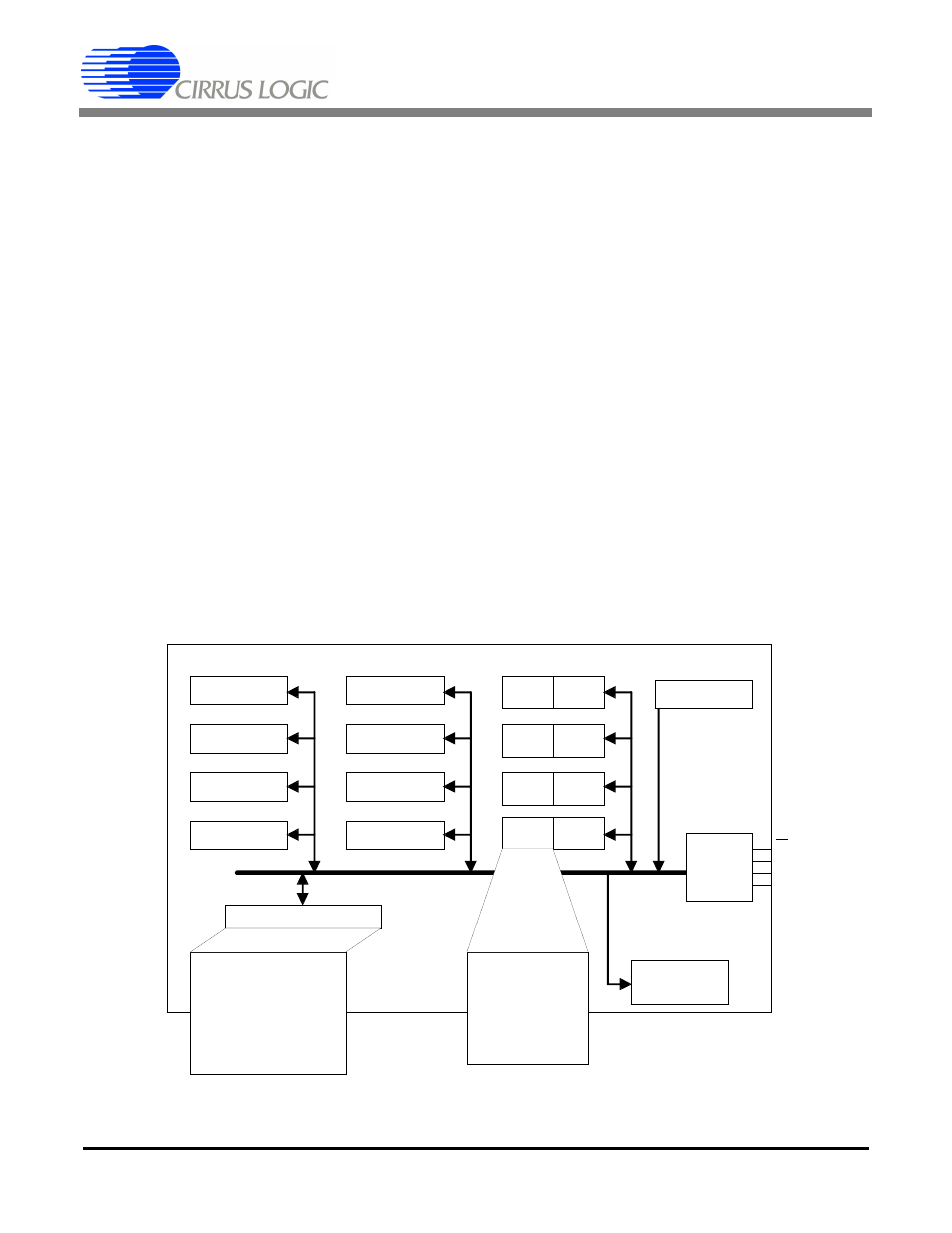
2.2. Overview of ADC Register Structure
and Operating Modes
The CS5531/32/33/34 ADCs have an on-chip con-
troller, which includes a number of user-accessible
registers. The registers are used to hold offset and
gain calibration results, configure the chip's operat-
ing modes, hold conversion instructions, and to
store conversion data words. Figure 6 depicts a
block diagram of the on-chip controller’s internal
registers.
Each of the converters has 32-bit registers to func-
tion as offset and gain calibration registers for each
channel. The converters with two channels have
two offset and two gain calibration registers, the
converters with four channels have four offset and
four gain calibration registers. These registers hold
calibration results. The contents of these registers
can be read or written by the user. This allows cal-
ibration data to be off-loaded into an external EE-
PROM. The user can also manipulate the contents
of these registers to modify the offset or the gain
slope of the converter.
The converters include a 32-bit configuration reg-
ister which is used for setting options such as the
power down modes, resetting the converter, short-
ing the analog inputs, and enabling diagnostic test
bits like the guard signal.
A group of registers, called Channel Setup Regis-
ters, are used to hold pre-loaded conversion in-
structions. Each channel setup register is 32 bits
long, and holds two 16-bit conversion instructions
referred to as Setups. Upon power up, these regis-
ters can be initialized by the system microcontrol-
ler with conversion instructions. The user can then
Offset 1 (1 x 32)
Offset 2 (1 x 32)
Offset 3 (1 x 32)
Offset 4 (1 x 32)
Gain 1 (1 x 32)
Gain 2 (1 x 32)
Gain 3 (1 x 32)
Gain 4 (1 x 32)
Setup 1
(1 x 16)
Setup 2
(1 x 16)
Setup 4
(1 x 16)
Setup 6
(1 x 16)
Setup 8
(1 x 16)
Setup 3
(1 x 16)
Setup 5
(1 x 16)
Setup 7
(1 x 16)
Offset Registers (4 x 32)
Gain Registers (4 x 32)
Channel Setup
Registers (4 x 32)
Conversion Data
Register (1 x 32)
Configuration Register (1 x 32)
Power Save Select
Reset System
Input Short
Guard Signal
Voltage Reference Select
Output Latch
Output Latch Select
Channel Select
Gain
W ord Rate
Unipolar/Bipolar
Output Latch
Delay Time
Open Circuit Detect
CS
SDI
SDO
SCLK
Read
O
n
ly
Com mand
Register (1 × 8)
Wr
it
e
O
n
ly
Serial
Interface
Data (1 x 32)
Offset/Gain Select
Filter Rate Select
Offset/Gain Pointer
Figure 6. CS5531/32/33/34 Register Diagram