Cirrus Logic CS5534-AS User Manual
Ultra-low-noise pgia, With, Features
Copyright
© Cirrus Logic, Inc. 2008
(All Rights Reserved)
CS5531/32/33/34-AS
16-bit and 24-bit ADCs
with
Ultra-low-noise PGIA
Features
Chopper-stabilized PGIA (Programmable
Gain Instrumentation Amplifier, 1x to 64x)
– 12 nV/
√Hz @ 0.1 Hz (No 1/f noise) at 64x
– 1200 pA Input Current with Gains >1
Delta-sigma Analog-to-digital Converter
– Linearity Error: 0.0007% FS
– Noise Free Resolution: Up to 23 bits
Two- or Four-channel Differential MUX
Scalable Input Span via Calibration
– ±5 mV to differential ±2.5V
Scalable V
REF
Input: Up to Analog Supply
Simple Three-wire Serial Interface
– SPI™ and Microwire™ Compatible
– Schmitt Trigger on Serial Clock (SCLK)
R/W Calibration Registers Per Channel
Selectable Word Rates: 6.25 to 3,840 Sps
Selectable 50 or 60 Hz Rejection
Power Supply Configurations
– VA+ = +5 V; VA- = 0 V; VD+ = +3 V to +5 V
– VA+ = +2.5 V; VA- = -2.5 V; VD+ = +3 V to +5 V
– VA+ = +3 V; VA- = -3 V; VD+ = +3 V
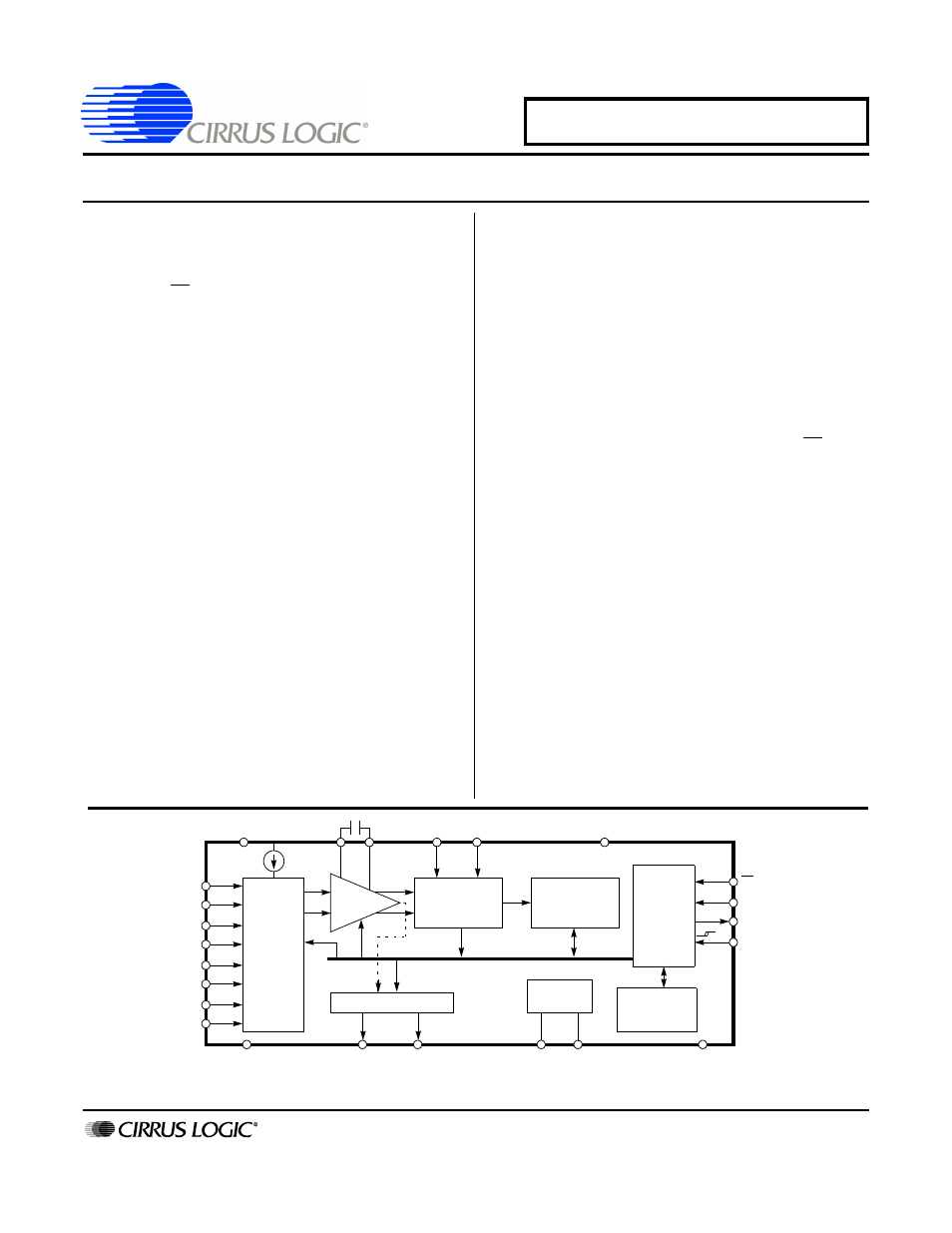
General Description
The CS5531/32/33/34 are highly integrated
∆Σ Analog-
to-Digital Converters (ADCs) which use charge-balance
techniques to achieve 16-bit (CS5531/33) and 24-bit
(CS5532/34) performance. The ADCs are optimized for
measuring low-level unipolar or bipolar signals in weigh
scale, process control, scientific, and medical
applications.
To accommodate these applications, the ADCs come as
either two-channel (CS5531/32) or four-channel
(CS5533/34) devices and include a very low noise chop-
per-stabilized instrumentation amplifier (6 nV/
√Hz @ 0.1
Hz) with selectable gains of 1Ч, 2Ч, 4Ч, 8Ч, 16Ч, 32Ч, and
64×. These ADCs also include a fourth order
∆Σ modu-
lator followed by a digital filter which provides twenty
selectable output word rates of 6.25, 7.5, 12.5, 15, 25, 30,
50, 60, 100, 120, 200, 240, 400, 480, 800, 960, 1600,
1920, 3200, and 3840 Sps (MCLK = 4.9152 MHz).
To ease communication between the ADCs and a micro-
controller, the converters include a simple three-wire se-
rial interface which is SPI and Microwire compatible with
a Schmitt-trigger input on the serial clock (SCLK).
High dynamic range, programmable output rates, and
flexible power supply options makes these ADCs ideal
solutions for weigh scale and process control
applications.
ORDERING INFORMATION
See
VA+
C1
C2
VREF+
VREF-
VD+
DIFFERENTIAL
4
TH
ORDER
∆Σ
MODULATOR
PGIA
1,2,4,8,16
PROGRAMMABLE
SINC FIR FILTER
MUX
(CS5533/34
SHOWN)
AIN1+
AIN1-
AIN2+
AIN2-
AIN3+
AIN3-
AIN4+
AIN4-
SERIAL
INTERFACE
LATCH
CLOCK
GENERATOR
CALIBRATION
SRAM/CONTROL
LOGIC
DGND
CS
SDI
SDO
SCLK
OSC2
OSC1
A1
A0/GUARD
VA-
32,64
OCT ‘08
DS289F5
Document Outline
- Features & Description
- Table of Contents
- List of Figures
- List of Tables
- 1. Characteristics And Specifications
- 2. General Description
- 2.1. Analog Input
- 2.2. Overview of ADC Register Structure and Operating Modes
- 2.3. Configuration Register
- 2.4. Setting up the CSRs for a Measurement
- 2.5. Calibration
- 2.6. Performing Conversions
- 2.7. Using Multiple ADCs Synchronously
- 2.8. Conversion Output Coding
- 2.9. Digital Filter
- 2.10. Clock Generator
- 2.11. Power Supply Arrangements
- 2.12. Getting Started
- 2.13. PCB Layout
- 3. Pin Descriptions
- 4. Soecification Definitions
- 5. Ordering Information
- 6. Environmental, Manufacturing, & Handling Information
- 7. Package Drawings