General description, Analog input, General description 2.1 – Cirrus Logic CS5534-AS User Manual
Page 12: Figure 3. multiplexer configuration
CS5531/32/33/34-AS
12
DS289F5
2. GENERAL DESCRIPTION
The CS5531/32/33/34 are highly integrated
∆Σ An-
alog-to-Digital Converters (ADCs) which use
charge-balance techniques to achieve 16-bit
(CS5531/33) and 24-bit (CS5532/34) performance.
The ADCs are optimized for measuring low-level
unipolar or bipolar signals in weigh scale, process
control, scientific, and medical applications.
To accommodate these applications, the ADCs
come as either two-channel (CS5531/32) or four-
channel (CS5533/34) devices and include a very-
low-noise, chopper-stabilized, programmable-gain
instrumentation amplifier (PGIA, 6 nV/
√Hz @ 0.1
Hz) with selectable gains of 1Ч, 2Ч, 4Ч, 8Ч, 16Ч,
32Ч, and 64×. These ADCs also include a fourth or-
der
∆Σ modulator followed by a digital filter which
provides twenty selectable output word rates of 6.25,
7.5, 12.5, 15, 25, 30, 50, 60, 100, 120, 200, 240, 400,
480, 800, 960, 1600, 1920, 3200, and 3840 Samples
per second (MCLK = 4.9152 MHz).
To ease communication between the ADCs and a
microcontroller, the converters include a simple
three-wire serial interface which is SPI and Mi-
crowire compatible with a Schmitt-trigger input on
the serial clock (SCLK).
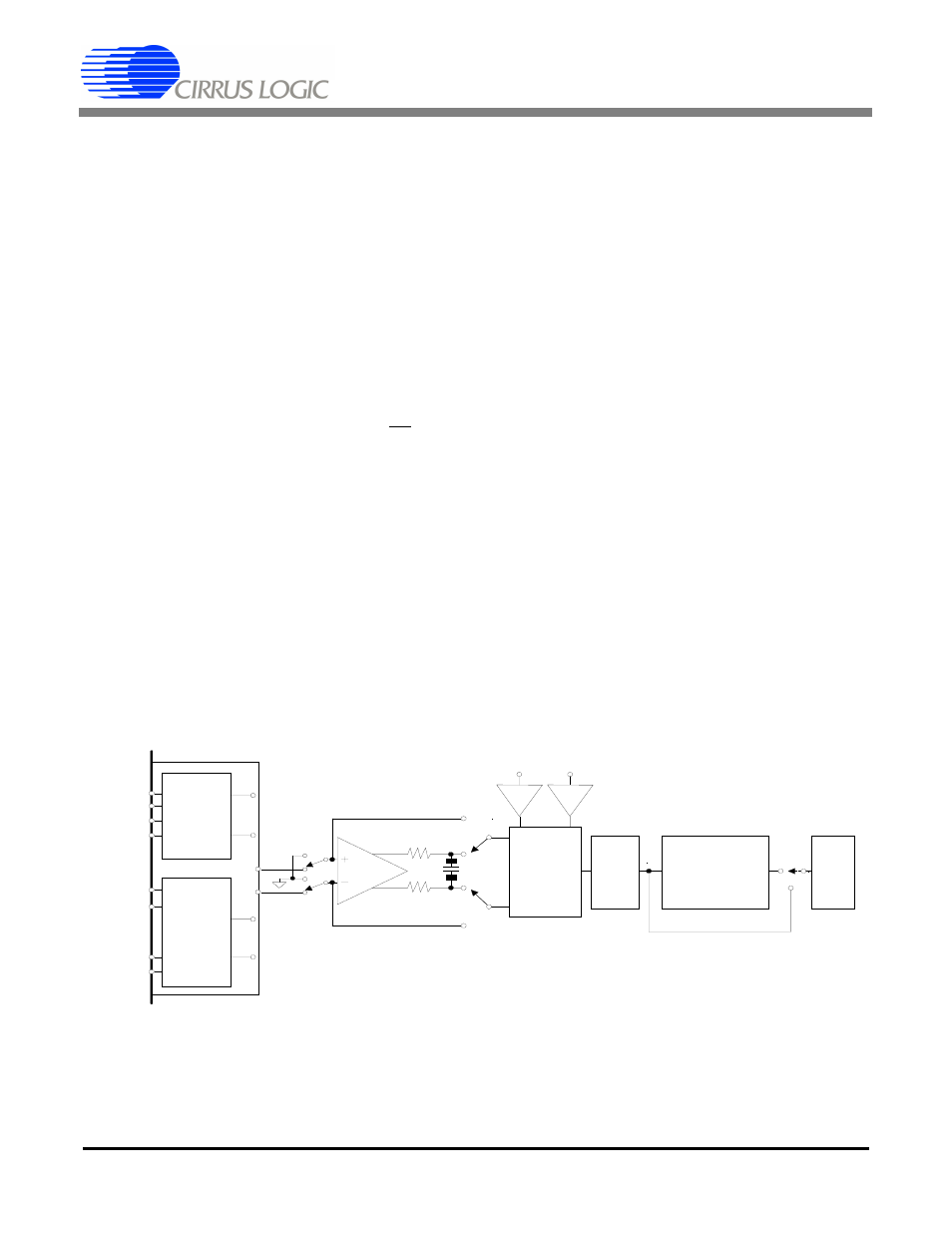
2.1. Analog Input
Figure 3 illustrates a block diagram of the
CS5531/32/33/34. The front end consists of a multi-
plexer, a unity gain coarse/fine charge input buffer,
and a programmable gain chopper-stabilized instru-
mentation amplifier. The unity gain buffer is activat-
ed any time conversions are performed with a gain
of one and the instrumentation amplifier is activated
any time conversions are performed with gain set-
tings greater than one.
The unity gain buffer is designed to accommodate
rail to rail input signals. The common-mode plus
signal range for the unity gain buffer amplifier is
VA- to VA+. Typical CVF (sampling) current for
the unity gain buffer amplifier is about 50 nA
(MCLK = 4.9152 MHz, see Figure 4).
The instrumentation amplifier is chopper stabilized
and operates with a chop clock frequency of
MCLK/128. The CVF (sampling) current into the
VREF+
Sinc
Digital
Filter
XGAIN
M
U
X
AIN2+
AIN2-
AIN1+
AIN1-
CS5531/32 IN+
IN-
AIN4+
AIN4-
*
*
*
AIN1+
AIN1-
CS5533/34
M
U
X
IN+
IN-
IN+
IN-
GAIN is the gain setting of the PGIA (i.e. 2, 4, 8, 16, 32, 64)
X1
X1
X1
VREF-
X1
Differential
4 Order
∆Σ
Modulator
th
5
Programmable
Sinc
Digital Filter
3
Serial
Port
1000
Ω
1000
Ω
22 nF
C1 PIN
C2 PIN
X 1
X 1
Figure 3. Multiplexer Configuration