Cirrus Logic CS5526 User Manual
Features, General description, Delta-sigma a/d converter
Copyright
© Cirrus Logic, Inc. 2005
(All Rights Reserved)
http://www.cirrus.com
CS5525
CS5526
16-bit/20-bit, Multi-range ADC with 4-bit Latch
Features
z
Delta-sigma A/D Converter
- Linearity Error: 0.0015%FS
- Noise-free Resolution: 18-bits
z
Bipolar/Unipolar Input Ranges
- 25 mV, 55 mV, 100 mV, 1 V, 2.5 V and 5 V
z
Chopper Stabilized Instrumentation Amplifier
z
On-chip Charge Pump Drive Circuitry
z
4-bit Output Latch
z
Simple three-wire serial interface
- SPI™ and Microwire™ Compatible
- Schmitt Trigger on Serial Clock (SCLK)
z
Programmable Output Word Rates
- 3.76 Sps to 202 Sps (XIN = 32.768 kHz)
- 11.47 Sps to 616 Sps (XIN = 100 kHz)
z
Output Settles in One Conversion Cycle
z
Simultaneous 50/60 Hz Noise Rejection
z
System and Self-calibration with
Read/Write Registers
z
Single +5 V Analog Supply
+3.0 V or +5 V Digital Supply
z
Low-power Mode Consumption: 4.9 mW
- 1.8 mW in 1 V, 2.5 V, and 5 V Input Ranges
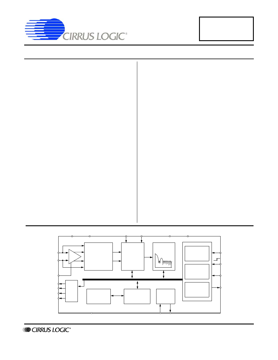
General Description
The 16-bit CS5525 and the 20-bit CS5526 are highly in-
tegrated
∆Σ A/D converters which include an
instrumentation amplifier, a PGA (programmable gain
amplifier), eight digital filters, and self and system cali-
bration circuitry.
The converters are designed to provide their own nega-
tive supply which enables their on-chip instrumentation
amplifiers to measure bipolar ground-referenced signals
≤±100 mV. By directly supplying NBV with -2.5 V and
with VA+ at 5 V,
±
2.5 V signals (with respect to ground)
can be measured.
The digital filters provide programmable output update
rates between 3.76 Sps to 202 Sps (XIN = 32.768 kHz).
Output word rates can be increased by approximately 3X
by using XIN = 100 kHz. Each filter is designed to settle
to full accuracy for its output update rate in one conver-
sion cycle. The filters with word rates of 15 Sps or less
(XIN = 32.768 kHz) reject both 50 and 60 Hz (
±
3 Hz) line
interference simultaneously.
Low power, single conversion settling time, programma-
ble output rates, and the ability to handle negative input
signals make these single supply products ideal solu-
tions for isolated and non-isolated applications.
ORDERING INFORMATION
See
AIN+
AIN-
+
-
X20
Programmable
Gain
VA+
AGND
VREF+
VREF-
VD+
DGND
XIN XOUT
SDO
SDI
NBV
A0
A1
A2
A3
Latch
Differential
Digital Filter
Calibration
Register
Control
Register
Output
Register
4th Order
Delta-Sigma
Modulator
Calibration
Memory
Calibration
µ
C
Clock
Gen.
SCLK
CS
CPD
AUG ‘05
DS202F5
Document Outline
- Features
- Characteristics & Specifications
- Detailed Description
- Theory of Operation
- System Initialization
- Command Operation
- Reading/Writing On-Chip Registers
- Analog Input
- Charge Pump Drive
- Voltage Reference
- Calibration
- Self Calibration
- System Calibration
- Calibration Tips
- Limitations in Calibration Range
- Analog Output Latch Pins
- Serial Port Interface
- Serial Port Initialization
- Performing Conversions (With PF bit = 0)
- Performing Conversions (With PF bit = 1)
- Output Word Rate Selection
- Clock Generator
- Digital Filter
- Output Coding
- Power Consumption
- PCB Layout
- Pin Descriptions
- Specification Definitions
- Ordering Information
- Environmental, Manufacturing, & Handling Information
- Revision History