Characteristics and specifications, Analog characteristics, Cs5509 – Cirrus Logic CS5509 User Manual
Page 2
CS5509
2
DS125F3
Notes: 1. Both source resistance and shunt capacitance are critical in determining the CS5509's source
impedance requirements. Refer to the text section Analog Input Impedance Considerations.
2. Specifications guaranteed by design, characterization and/or test.
3. Applies after calibration at the temperature of interest.
4. Total drift over the specified temperature range since calibration at power-up at 25 °C.
5. The input is differential. Therefore, GND
≤ Signal + Common Mode Voltage ≤ VA+.
6. The CS5509 can accept input voltages up to the VA+ analog supply. In unipolar mode the CS5509 will
output all 1's if the dc input magnitude ((AIN+) - (AIN-)) exceeds ((VREF+) - (VREF-)) and will output all
0's if the input becomes more negative than 0 Volts. In bipolar mode the CS5509 will output all 1's if the
dc input magnitude ((AIN+) - (AIN-)) exceeds ((VREF+) - (VREF-)) and will output all 0's if the input
becomes more negative in magnitude than -((VREF+) - (VREF-)).
7. All outputs unloaded. All inputs CMOS levels.
* Refer to the Specification Definitions immediately following the Pin Description Section.
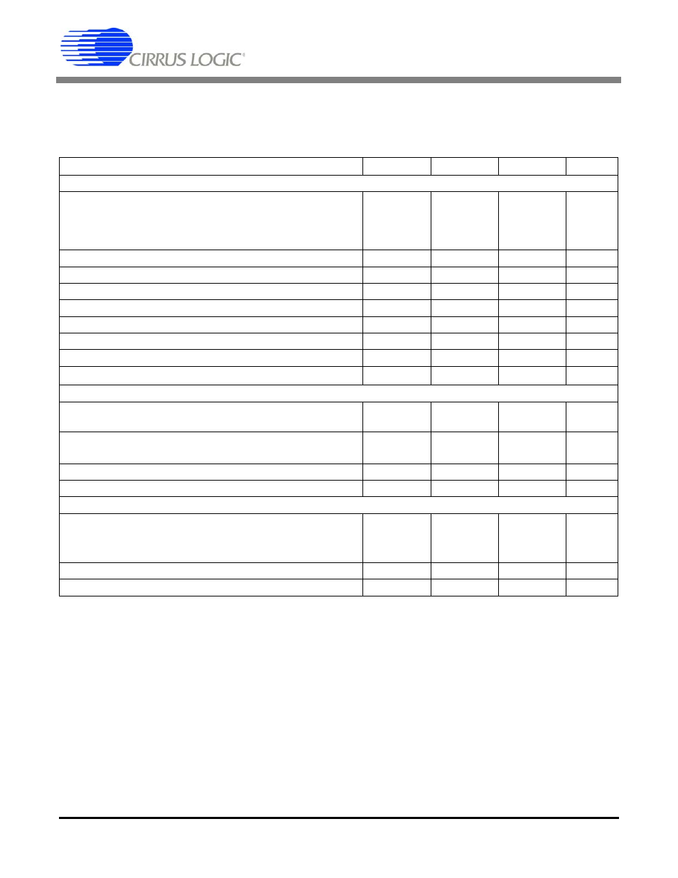
ANALOG CHARACTERISTICS
(T
A
= 25 °C; VA+ = 5V ±5%; VD+ = 3.3V ±5%; VREF+ = 2.5V,
VREF- = 0V; f
CLK
= 32.768 kHz; Bipolar Mode; R
source
= 40
Ω with a 10 nF to GND at AIN; AIN- = 2.5V; unless oth-
erwise specified.) (Notes 1 and 2)
Parameter*
Min Typ
Max
Unit
Accuracy
Linearity Error
f
CLK
= 32.768 kHz
f
CLK
= 165 kHz
f
CLK
= 247.5 kHz
f
CLK
= 330 kHz
-
-
-
-
0.0015
0.0015
0.0015
0.005
0.003
0.003
0.003
0.0125
± %FS
± %FS
± %FS
± %FS
Differential Nonlinearity
-
±0.25
±0.5
LSB
Full-scale Error
(Note 3)
-
±0.25
±2
LSB
Full-scale Drift
(Note 4)
-
±0.5
-
LSB
Unipolar Offset
(Note 3)
-
±0.5
±2
LSB
Unipolar Offset Drift
(Note 4)
-
±0.5
-
LSB
Bipolar Offset
(Note 3)
-
±0.25
±1
LSB
Bipolar Offset Drift
(Note 4)
-
±0.25
-
LSB
Noise (Referred to Output)
-
0.16
-
LSB
rms
Analog Input
Analog Input Range
Unipolar
Bipolar
(Notes 5 and 6)
-
-
0 to +2.5
±2.5
-
-
V
V
Common Mode Rejection
dc
f
CLK
= 32.768 kHz
50, 60 Hz
(Note 2)
-
120
105
-
-
-
dB
dB
Input Capacitance
-
15
-
pF
DC Bias Current
(Note 1)
-
5
-
nA
Power Supplies
DC Power Supply Currents
I
Total
I
Analog
I
Digital
-
-
-
350
300
60
450
-
-
µA
µA
µA
Power Dissipation
(Note 7)
-
1.7
2.25
mW
Power Supply Rejection
-
80
-
dB