Pin descriptions, Cs5509 – Cirrus Logic CS5509 User Manual
Page 19

CS5509
DS125F3
19
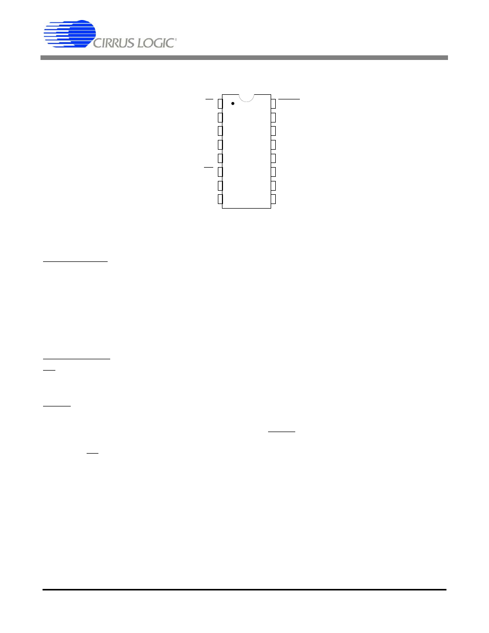
PIN DESCRIPTIONS*
* Pinout applies to both PDIP and SOIC
Clock Generator
XIN; XOUT - Crystal In; Crystal Out, Pins 4, 5.
A gate inside the chip is connected to these pins and can be used with a crystal to provide the
master clock for the device. Alternatively, an external (CMOS compatible) clock can be
supplied into the XIN pin to provide the master clock for the device. Loss of clock will put the
device into a lower powered state (approximately 70% power reduction).
Serial Output I/O
CS - Chip Select, Pin 1.
This input allows an external device to access the serial port.
DRDY - Data Ready, Pin 16.
Data Ready goes low at the end of a digital filter convolution cycle to indicate that a new
output word has been placed into the serial port. DRDY will return high after all data bits are
shifted out of the serial port or two master clock cycles before new data becomes available if
the CS pin is inactive (high).
SDATA - Serial Data Output, Pin 15.
SDATA is the output pin of the serial output port. Data from this pin will be output at a rate
determined by SCLK. Data is output MSB first and advances to the next data bit on the falling
edges of SCLK. SDATA will be in a high impedance state when not transmitting data.
SCLK - Serial Clock Input, Pin 14.
A clock signal on this pin determines the output rate of the data from the SDATA pin. This pin
must not be allowed to float.
1
2
3
4
5
6
7
8
9
10
11
12
13
14
15
16
DRDY
SDATA
SCLK
VD+
GND
VA+
VREF-
VREF+
AIN-
AIN+
BP/UP
XOUT
XIN
CAL
CONV
CS
DIFFERENTIAL ANALOG INPUT
DIFFERENTIAL ANALOG INPUT
BIPOLAR / UNIPOLAR
CRYSTAL OUT
CRYSTAL IN
CALIBRATE
CONVERT
CHIP SELECT
DATA READY
SERIAL DATA OUTPUT
SERIAL CLOCK INPUT
POSITIVE DIGITAL POWER
GROUND
POSITIVE ANALOG POWER
VOLTAGE REFERENCE INPUT
VOLTAGE REFERENCE INPUT
