Digital filter characteristics, Cs5509 – Cirrus Logic CS5509 User Manual
Page 13
CS5509
DS125F3
13
An equation for the maximum acceptable source
resistance is derived.
This equation assumes that the offset voltage of the
buffer is 100 mV, which is the worst case. The val-
ue of Ve is the maximum error voltage which is ac-
ceptable. C
EXT
is the combination of any external
or stray capacitance.
For a maximum error voltage (Ve) of 10 µV in the
CS5509 (1/4LSB at 16-bits), the above equation in-
dicates that when operating from a 32.768 kHz
XIN, source resistances up to 110 k
Ω are accept-
able in the absence of external capacitance
(C
EXT
=0).
The VREF+ and VREF- inputs have nearly the
same structure as the AIN+ and AIN- inputs.
Therefore, the discussion on analog input imped-
ance applies to the voltage reference inputs as well.
Digital Filter Characteristics
The digital filter in the CS5509 is the combination
of a comb filter and a low pass filter. The comb fil-
ter has zeros in its transfer function which are opti-
mally placed to reject line interference frequencies
(50 and 60 Hz and their multiples) when the
CS5509 is clocked at 32.768 kHz. Figures 6, 7 and
8 illustrate the magnitude and phase characteristics
of the filter. Figure 6 illustrates the filter attenua-
tion from dc to 260 Hz. At exactly 50, 60, 100, and
120 Hz the filter provides over 120 dB of rejection.
Table 2 indicates the filter attenuation for each of
the potential line interference frequencies when the
converter is operating with a 32.768 kHz clock.
The converter yields excellent attenuation of these
interference frequencies even if the fundamental
line frequency should vary ± 1% from its specified
frequency. The -3 dB corner frequency of the filter
when operating from a 32.768 kHz clock is 17 Hz.
Figure 8 illustrates that the phase characteristics of
the filter are precisely linear phase.
If the CS5509 is operated at a clock rate other than
32.768kHz, the filter characteristics, including the
comb filter zeros, will scale with the operating
clock frequency. Therefore, optimum rejection of
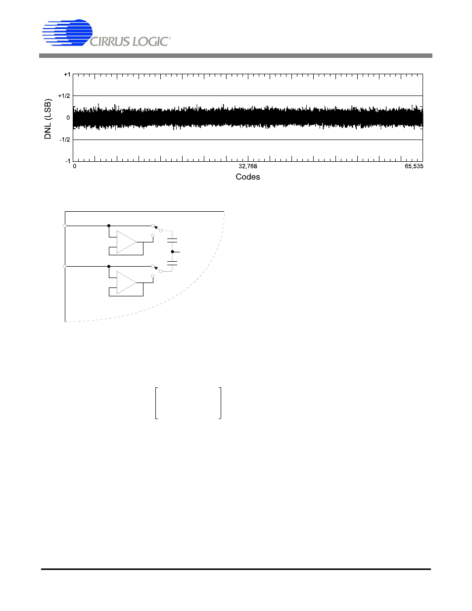
Figure 4. CS5509 Differential Nonlinearity Plot
+
15 pF
V
os
≤ 100 mV
+
V
os
≤ 100 mV
Internal
Bias
Voltage
15 pF
AIN+
AIN-
-
-
Figure 5. Analog Input Model
Rs
max
1
–
2XIN 15pF
C
EXT
+
(
)
V
e
V
e
15pF 100mV
(
)
15pF
C
EXT
+
-------------------------------------
+
---------------------------------------------------
ln
-------------------------------------------------------------------------------------------------------------------------
=