3v switching characteristics – Cirrus Logic CS5508 User Manual
Page 7
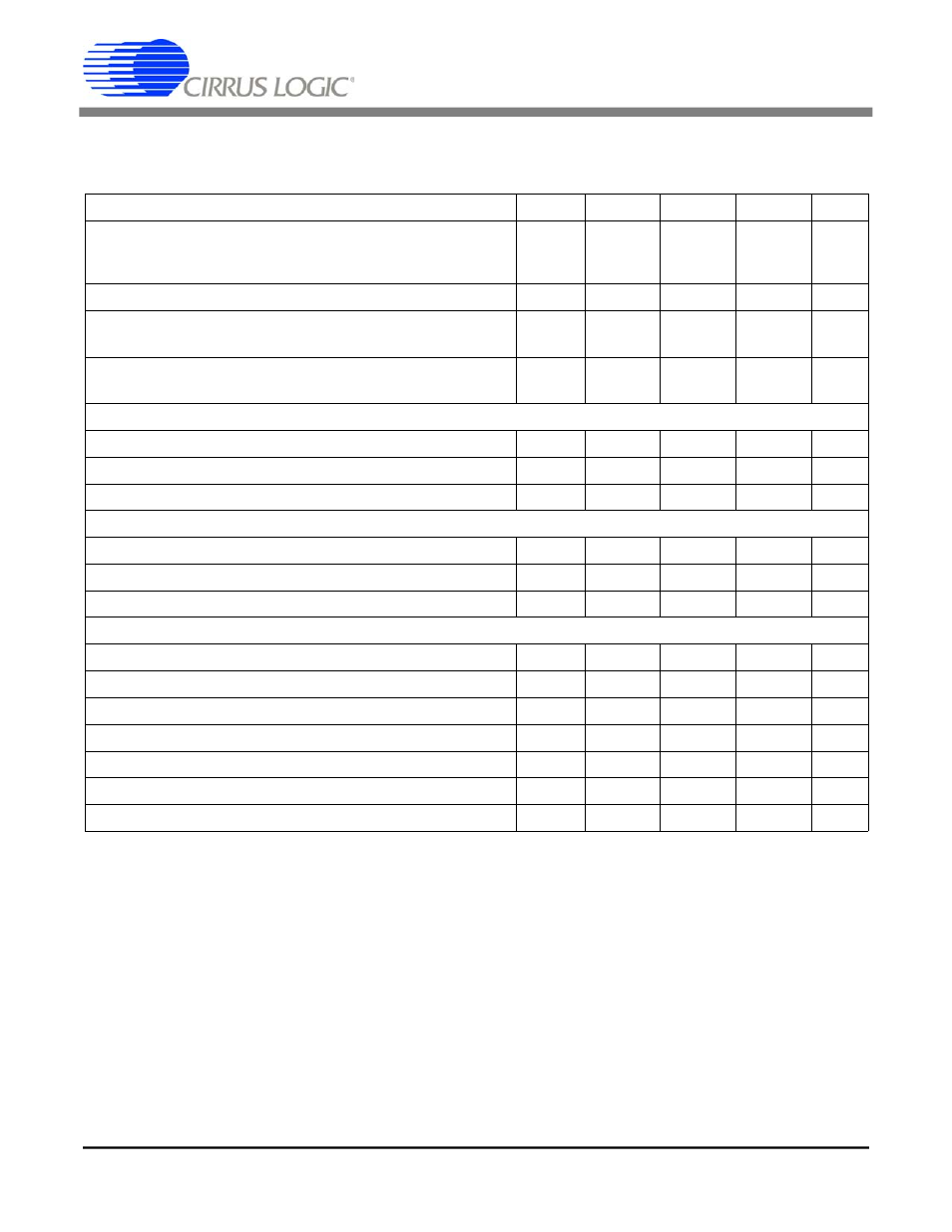
3.3V SWITCHING CHARACTERISTICS
(T
A
= T
MIN
to T
MAX
VA+ = 5V
± 10%;
VD+ = 3.3V
± 5%; VA- = -5V ± 10%; Input Levels: Logic 0 = 0V, Logic 1 = VD+; CL = 50 pF.) (Note 2)
Parameter
Symbol
Min
Typ
Max
Units
Master Clock Frequency:
Internal Oscillator:
-A,B
-S
External Clock:
XIN
or
f
clk
30.0
30.0
30
32.768
32.768
-
53.0
34.0
163
kHz
kHz
kHz
Master Clock Duty Cycle
40
-
60
%
Rise Times:
Any Digital Input
(Note 10)
Any Digital Output
t
rise
-
-
-
50
1.0
-
µs
ns
Fall Times:
Any Digital Input
(Note 10)
Any Digital Output
t
fall
-
-
-
20
1.0
-
µs
ns
Start-Up
Power-On Reset Period
(Note 11)
t
res
-
10
-
ms
Oscillator Start-up Time
XTAL=32.768 kHz (Note 12)
t
osu
-
500
-
ms
Wake-up Period
(Note 13)
t
wup
-
1800/f
clk
-
s
Calibration
CONV Pulse Width (CAL = 1)
(Note 14)
t
ccw
100
-
-
ns
CONV and CAL High to Start of Calibration
t
scl
-
-
2/f
clk+
200
ns
Start of Calibration to End of Calibration
t
cal
-
3246/f
clk
-
s
Conversion
Set Up Time
A0, A1 to CONV High
t
sac
50
-
-
ns
Hold Time
A0, A1 after CONV High
t
hca
100
-
-
ns
CONV Pulse Width
t
cpw
100
-
-
ns
CONV High to Start of Conversion
t
scn
-
-
2/f
clk
+200
ns
Set Up Time
BP/UP stable prior to DRDY falling
t
bus
82/f
clk
-
-
s
Hold Time
BP/UP stable after DRDY falls
t
buh
0
-
-
ns
Start of Conversion to End of Conversion
(Note 15)
t
con
-
1624/f
clk
-
s
CS5505/6/7/8
DS59F4
7
CS5505/6/7/8
DS59F7
7