Schematic & layout review service – Cirrus Logic CS5508 User Manual
Page 25
CS5505/6
+10V
Analog
Supply
VD+
VA+
M/SLP
SCLK
SDATA
CAL
VREF+
VREF-
DGND
VA-
DRDY
CS
A0
A1
BP/UP
AIN1+
AIN-
AIN2+
AIN3+
AIN4+
CONV
Note:
XIN
XOUT
(1) To use the internal 2.5 volt reference see Figure 6.
(2) VD+ must never exceed VA+. Examine power-up conditions.
*Unused analog inputs
should be tied to AIN-
0.1
µF
0.1
µF
4
8
13
12
11
10
9
14
15
1
2
3
5
6
7
17
18
19
20
21
22
23
24
Analog*
Signal
Sources
Signal
Ground
32.768 kHz
Voltage
Reference
16
VREFOUT
+
-
Calibration
Control
Bipolar/
Unipolar
Input Select
Unused Logic
inputs must be
connected to
VD+ or DGND.
Control
Logic
Serial
Data
Interface
Sleep Mode
Control
and
Output Mode
Select
Optional
Clock
Source
(1)
+5V
Analog
Supply
(2)
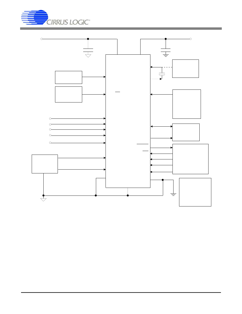
Figure 16. CS5505/6 System Connection Diagram Using External Reference,
Dual Supply, +10V Analog, +5V Digital
Schematic & Layout Review Service
Confirm Optimum
Schematic & Layout
Before Building Your Board.
Confirm Optimum
Schematic & Layout
Before Building Your Board.
For Our Free Review Service
Call Applications Engineering.
For Our Free Review Service
Call Applications Engineering.
C a l l : ( 5 1 2 ) 4 4 5 - 7 2 2 2
CS5505/6/7/8
DS59F4
25
CS5505/6/7/8
DS59F7
25