Cirrus Logic CS5508 User Manual
Page 23
analog ground pin. No analog ground pin is re-
quired because the inputs for measurement and
for the voltage reference are differential and re-
quire no ground. In the digital section of the
chip the supply current flows into the VD+ pin
and out of the DGND pin. As a CMOS device,
the CS5505/6/7/8 requires that the supply volt-
age on the VA+ pin always be more positive
than the voltage on any other pin of the device.
If this requirement is not met, the device can
latch-up or be damaged. In all circumstances the
VA+ voltage must remain more positive than the
VD+ or DGND pins; VD+ must remain more
positive than the DGND pin.
The following power supply options are possi-
ble:
VA+ = +5V to +10V, VA- = 0V,
VD+ = +5V
VA+ = +5V,
VA- = -5V,
VD+ = +5V
VA+ = +5V ,
VA- = 0V to -5V,
VD+ = +3.3V
The CS5505/6/7/8 cannot be operated with a
3.3V digital supply if VA+ is greater than
+5.5V.
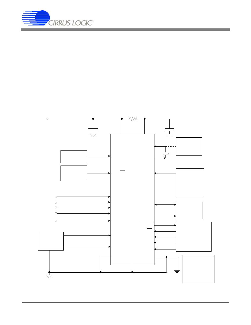
CS5505/6
+5V
Analog
Supply
VD+
10
Ω
VA+
M/SLP
SCLK
SDATA
CAL
VREF+
VREF-
DGND
VA-
DRDY
CS
A0
A1
BP/UP
AIN1+
AIN-
AIN2+
AIN3+
AIN4+
CONV
Note:
XIN
XOUT
To use the internal 2.5 volt reference see Figure 6.
*Unused analog inputs
should be tied to AIN-
0.1
µF
0.1
µF
4
8
13
12
11
10
9
14
15
1
2
3
5
6
7
17
18
19
20
21
22
23
24
Analog*
Signal
Sources
Signal
Ground
32.768 kHz
Voltage
Reference
16
VREFOUT
+
-
Calibration
Control
Bipolar/
Unipolar
Input Select
Unused Logic
inputs must be
connected to
VD+ or DGND.
Control
Logic
Serial
Data
Interface
Sleep Mode
Control
and
Output Mode
Select
Optional
Clock
Source
Figure 14. CS5505/6 System Connection Diagram Using External Reference, Single Supply
CS5505/6/7/8
DS59F7
23
CS5505/6/7/8
DS59F7
23