Cirrus Logic CS5508 User Manual
Page 24
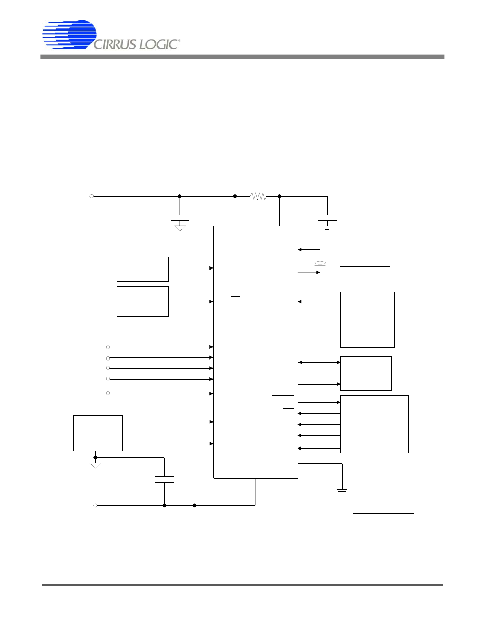
Figure 14 illustrates the System Connection Dia-
gram for the CS5505/6 using a single +5V
supply. Note that all supply pins are bypassed
with 0.1
µF capacitors and that the VD+ digital
supply is derived from the VA+ supply.
Figure 15 illustrates the CS5505/6 using dual
supplies of +5 and -5V.
Figure 16 illustrates the CS5505/6 using dual
supplies of +10V analog and +5V digital.
When using separate supplies for VA+ and
VD+, VA+ must be established first. VD+
should never become more positive than VA+
under any operating condition. Remember to in-
vestigate transient power-up conditions, when
one power supply may have a faster rise time.
CS5505/6
+5V
Analog
Supply
VD+
10
Ω
VA+
M/SLP
SCLK
SDATA
CAL
VREF+
VREF-
DGND
VA-
DRDY
CS
A0
A1
BP/UP
AIN1+
AIN-
AIN2+
AIN3+
AIN4+
CONV
Note:
XIN
XOUT
To use the internal 2.5 volt reference see Figure 6.
*Unused analog inputs
should be tied to AIN-
0.1
µF
0.1
µF
4
8
13
12
11
10
9
14
15
1
2
3
5
6
7
17
18
19
20
21
22
23
24
Analog*
Signal
Sources
Signal
Ground
32.768 kHz
Voltage
Reference
16
VREFOUT
+
-
Calibration
Control
Bipolar/
Unipolar
Input Select
Unused Logic
inputs must be
connected to
VD+ or DGND.
Control
Logic
Serial
Data
Interface
Sleep Mode
Control
and
Output Mode
Select
Optional
Clock
Source
0.1
µF
-5V
Analog
Supply
Figure 15. CS5505/6 System Connection Diagram Using External Reference, Dual Supplies
CS5505/6/7/8
24
DS59F7
CS5505/6/7/8
24
DS59F7