Cirrus Logic AN31 User Manual
Page 19
nominal. In other words, the gain can be
calibrated for an input as low as 10 mV or as
high as 15 mV when the nominal value is set for
12.5 mV. The nominal input can be changed by
changing the PGA gain or by changing the
divider resistors for the excitation voltage. The
converter can accept a VREF input voltage of
any value between 2.0 to 3.8 V. The CS5516
and CS5520 can be operated on any clock
frequency from 1.0 MHz to 5.0 MHz. The
digital filter will give greater than 90 dB of
attenuation to 50 and 60 Hz line interference if
the input clock is 4.096 mHz or less. With a
4.096 MHz clock into the converter it will
output conversion words at a 50 Hz rate. For
optimal filtering it is desirable to average output
words from the converter. If ten output words
are averaged, the noise bandwidth is reduced to
about 2.5 Hz.
CS5516 with External 25 Hz AC Excitation
The CS5516 and CS5520 support two ac bridge
excitation modes; internal and external. In the
internal excitation mode, the excitation clock is
derived internal to the converter from the
oscillator frequency on the chip and is output
from the BX1 and BX2 pins. In the external
excitation mode (selected by setting a bit in the
configuration register of the converter), a square
wave whose frequency is a sub-multiple of the
XIN frequency to the converter (see the
CS5516/20 data sheet for details) is input into
the BX1 pin of the converter.
When using the CS5516 or CS5520 in the ac
excitation mode, the AIN and VREF signals into
the converter are sampled 64 XIN clock cycles
after the excitation signal is switched. When the
square wave excitation changes polarity, the
circuitry, including the bridge, the load cell
cable, and any filtering components must settle
to at least 5 per cent accuracy within the 64 XIN
clock cycles after the switching edge. This can
be a limiting factor in using square wave ac
excitation, especially with long cables which
have a large capacitance.
The excitation frequency can be lowered to
XIN/(10 X 2
14
) if output words from the
converter are averaged over several conversion
cycles. For example, with a 4.096 MHz clock, a
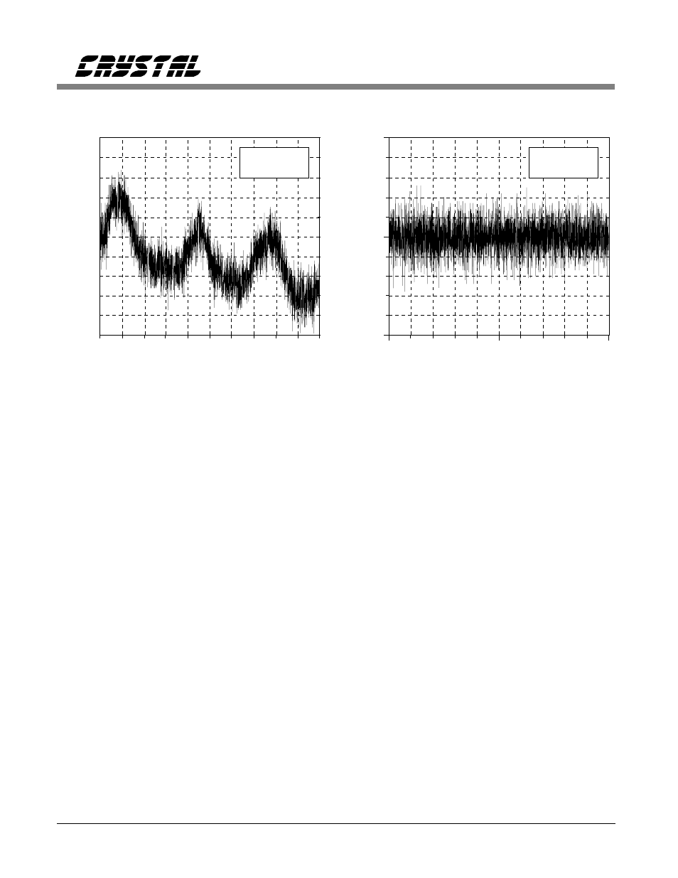
0.00
0.50
1.00
DC Excitation
Time Domain Data
time (hours)
0.00
0.50
1.00
AC Excitation
Time Domain Data
time (hours)
Nanovolts
1250
1000
750
-500
250
0
-250
500
-750
-1000
-1250
Nanovolts
1250
1000
750
-500
250
0
-250
500
-750
-1000
-1250
1 LSB = 25 nV
1 LSB = 25 nV
Figure 14. DC Versus AC Excitation.
Bridge Transducer Digitizer Circuits
AN31REV3
19