2 digital section, 1 current channel gain, Cdb5466u – Cirrus Logic CDB5466U User Manual
Page 5: Vref

CDB5466U
DS676DB1
5
to position VIN+, J22 to position VN-, J24 to position IIN+ and J26 to position IIN-, the input voltage signal is supplied
from the screw terminals J23 and J27. With a jumper on J17, J22, J24 and J26 in the GND position, the inputs are
connected to analog ground (AGND). With a jumper on J17, J22, J24 and J26 in position
VREF
, the inputs are con-
nected to the reference voltage selected on J12.
1.2.2
Digital Section
The digital section contains the microcontroller, USB interface, JTAG header, reset circuitry, and an external inter-
face header (J11). The microcontroller interfaces the energy pulses, E1, E2, and FOUT output by the CS5466 with
the USB connection to the PC. The microcontroller also provides a hardware reset to the CS5466, which is level
shifted to support both +3.3 V and +5 V digital operation. Interface header, J11, is provided to allow the CDB5466U
to be connected to an external energy registration device. The energy output pins E1, E2, FOUT and NEG are routed
to LEDs which provide a simple visual check of the energy output pulses. Jumpers J10, J13, J15 and J16 are
equipped at the factory with jumpers to enable the LEDs.
1.2.2.1
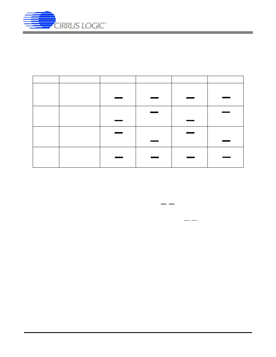
Current Channel Gain
To accommodate different current-sensing elements the current channel incorporates a programmable gain that can
be set to one of four input ranges. Input pins IGAIN1 and IGAIN0 define the four gain selections and corresponding
maximum input signal level. Jumpers J31 and J32 define the state of IGAIN1 and IGAIN0, respectively. Table 4 il-
lustrates the options available. With jumpers J31 = J32 = GND the gain is set to 10x. With jumpers J31 = GND and
J32 = VD+ the gain is set to 50x. With jumpers J31 = VD+ and J32 = GND the gain is set to 100x. With jumpers
J31 = VD+ and J32 = VD+ the gain is set to 150x.
INPUT
Description
J17
J22
J24
J26
VIN± or IIN±
Selects External
Signal
VIN± or IIN±
Selects External
Signal
GND
Selects Grounding
the Input
VREFIN
Selects Reference
Source
Table 3. Voltage and Current Channel Input Signal Selection
O
VIN+
O O
VIN+
O O
VIN+
GND
VREF
VIN+
(Default)
O
VIN-
O O
VIN-
O O
VIN-
VIN-
VREF
GND
(Default)
O
IIN+
O O
IIN+
O O
IIN+
GND
VREF
IIN+
(Default)
O
IIN-
O O
IIN-
O O
IIN-
IIN-
VREF
GND
(Default)
O
VIN+
O O
VIN+
O O
VIN+
GND
VREF
VIN+
O
VIN-
O O
VIN-
O O
VIN-
VIN-
VREF
GND
O
IIN+
O O
IIN+
O O
IIN+
GND
VREF
IIN+
O
IIN-
O O
IIN-
O O
IIN-
IIN-
VREF
GND
O
VIN+
O O
VIN+
O O
VIN+
GND
VREF
VIN+
O
VIN-
O O
VIN-
O O
VIN-
VIN-
VREF
GND
O
IIN+
O O
IIN+
O O
IIN+
GND
VREF
IIN+
O
IIN-
O O
IIN-
O O
IIN-
IIN-
VREF
GND
O
VIN+
O O
VIN+
O O
VIN+
GND
VREF
VIN+
O
VIN-
O O
VIN-
O O
VIN-
VIN-
VREF
GND
O
IIN+
O O
IIN+
O O
IIN+
GND
VREF
IIN+
O
IIN-
O O
IIN-
O O
IIN-
IIN-
VREF
GND
