Hardware, 1 introduction, 2 evaluation board overview – Cirrus Logic CDB5466U User Manual
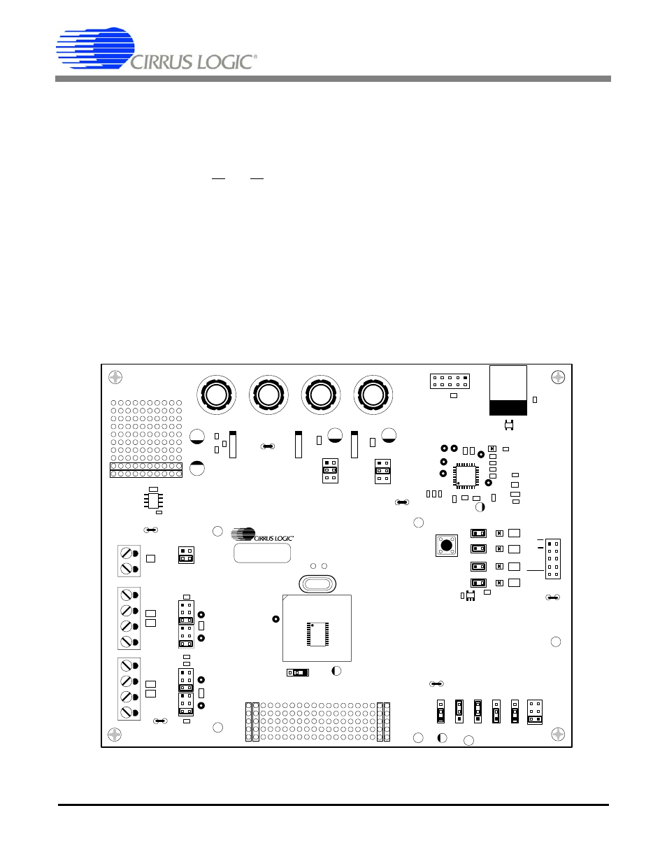
Page 3: 1 introduction 1.2 evaluation board overview, Figure 1. cdb5466u assembly drawing, Cdb5466u, Hardware 1.1 introduction

CDB5466U
DS676DB1
3
1. HARDWARE
1.1
Introduction
The CS5466 is a low cost power measurement solution combining two
∆Σ analog-to-digital converters (ADCs), an
energy-to-frequency converter, and energy pulse outputs on a single chip. It is designed to accurately measure and
calculate energy for single phase, 2- or 3-wire power metering applications with minimal external components.
Low-frequency energy outputs, E1 and E2 supply average active power and can be used to drive a stepper motor
or a mechanical counter; the high-frequency energy output FOUT is designed to assist in calibration; and NEG in-
dicates negative energy.
The CS5466 has configuration pins which allow the selection of pulse output frequency, current channel input range,
and the high-pass filter enable option. The CS5466 also has a power-on reset function which holds the part in reset
until the supply reaches the proper level. The CDB5466U is shipped with a CS5466-ISZ device located at U6.
1.2
Evaluation Board Overview
The CDB5466U evaluation board provides a quick path to evaluating the CS5466 Power Measurement IC. Figure
1 illustrates the placement of the terminals, jumpers and IC components. The jumper options are shown in the fac-
tory default positions.
Figure 1. CDB5466U Assembly Drawing
CDB5466U REV X
JTAG
USB
J2
J6
Vu+_EXT
VD+_EXT
GND
+5V
J5
J4
J3
VIN+
VIN-
TP9
TP11
IIN+
IIN-
TP12
TP13
JP6
GND
GND
VREF
VIN+
VIN-
VREF
GND
GND
VREF
IIN+
IIN-
VREF
GND
GND
IIN+
IIN-
GND
GND
VIN+
VIN-
GND
REF+
GND
JP3
GND
J17
J22
J24
J26
J12
LT1019
REF+
J8
VD+_EXT
+5V
J9
+3.3V
VD+
Vu+_EXT
+5V
VD+
8051_REGIN
JP1
GND
JP2
GND
TP1 TP2
TP4
TP5
TP3
TP6
J10
1
J13
1
J15
1
J16
1
LED_EN
LED_EN
LED_EN
LED_EN
E1
E2
FOUT
NEG
J11
E1
E2
FOUT
NEG
RESET
GND
EXT EN
ER
R
E
G
GND
JP4
J32
J31
J30
J29
J28
JP5
GND
TP10
CPUCLK
U7
Y1
J25
VR
E
F
VR
E
FI
N
V
RE
FOUT
VA+GND
VD+
GND
J14
J23
J27
GND
VD+
5466
J33
FOUT
GND
VD+
IGAIN0
IGAIN1
FREQ0
FREQ1
FREQ2
HPF
CS5466 CONFIG
RESET
S1
4.096MHz
TP7
TP8
XOUT XIN
U3
8051
U4
U5
J1
