1 analog section, Cdb5466u – Cirrus Logic CDB5466U User Manual
Page 4

CDB5466U
4
DS676DB1
The CDB5466U evaluation board is partitioned into two main sections - analog and digital. The analog section con-
sists of the CS5466 and a precision voltage reference that operates from a single +5 V power supply. The digital
section consists of the microcontroller, the reset circuitry, and the USB interface. The digital section can operate from
a +5 V or +3.3 V power supply. The evaluation board is epuipped with power supply connections that accommodate
all of the various supply options of the CS5466.
The evaluation board is designed to output energy-to-pulse conversions upon power-up. Software that runs on a PC
provides a GUI (Graphical User Interface) as a means to quickly register and evaluate the CS5466’s energy-to-pulse
outputs. To accomplish this, the board comes equipped with USB drivers and cable which physically interfaces the
evaluation board to the PC. The software provides easy access to the energy outputs E1, E2, and FOUT and pro-
vides a means to display and evaluate the performance of the CS5466.
1.2.1
Analog Section
The CDB5466U evaluation board provides screw-type terminals (J23 and J27) to connect input signals to the volt-
age and current channels. The screw terminals are labeled as VIN+, VIN-, IIN+, and IIN-. A simple R-C network at
each channel input provides a simple anti-alias filter.
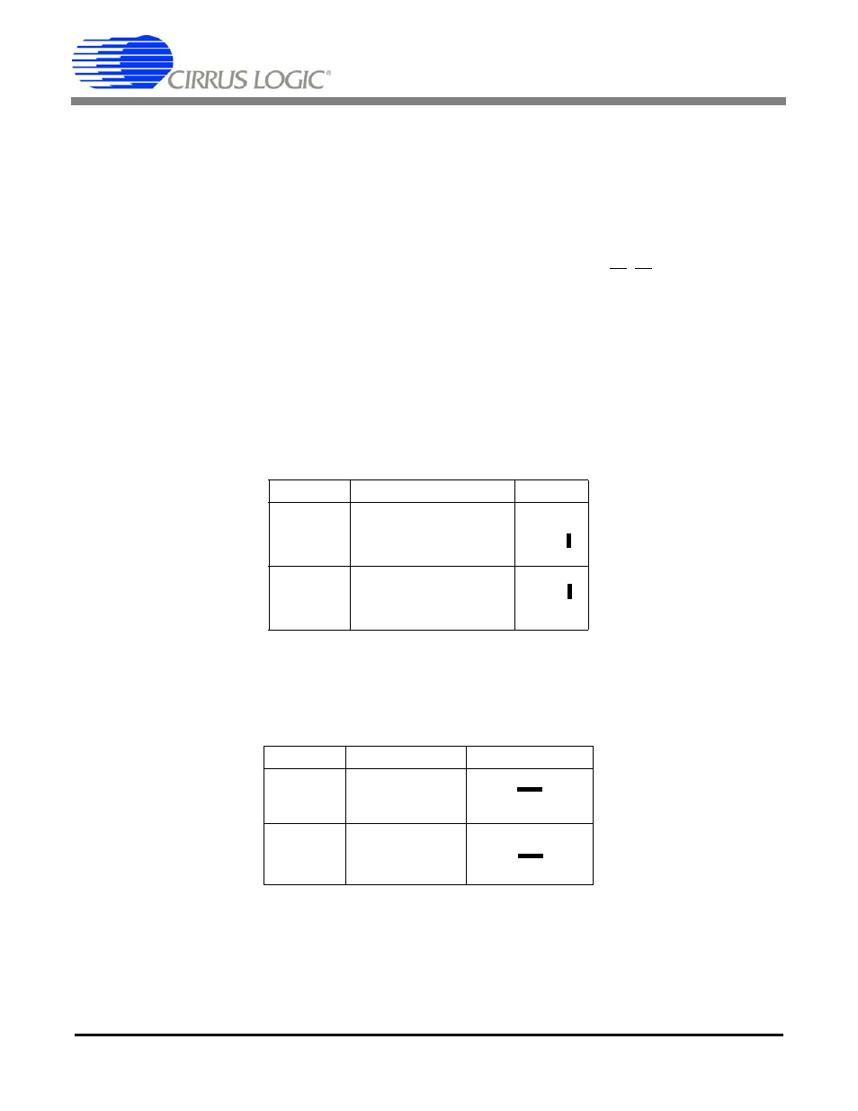
The evaluation board provides three voltage reference options for VREFIN to the CS5466. The three voltage refer-
ence options include: VREFOUT from the CS5466, the on-board +2.5 V reference, and external REF+ (screw ter-
minal J14). Table 1 and Table 2 illustrate the options available for VREFIN. With a jumper on J25 in the position
labeled VREFOUT, the reference is supplied by the on-chip voltage reference. With a jumper on J25 in the position
labeled VREF, the reference is supplied by an off-chip voltage reference.
Table 2 illustrates the options available for VREF. With a jumper on J12 in position LT1019, the LT1019 provides a
+2.5 V reference (the LT1019 was chosen for its low drift - typically 5ppm/°C). By setting the jumper on J12 to posi-
tion REF+, an external voltage reference is supplied via screw terminal J14’s REF+ input.
The three input signal options for the voltage (VIN±) and current (IIN±) channel input include: an external signal
(screw terminals J23 and J27), GND or VREF. Table 3 illustrates the options available. By installing jumpers on J17
Reference
Description
J25
VREFOUT
Selects on-Chip
Reference (25ppm/
°
C)
VREF
Selects External or
LT1019 Reference(J12)
Table 1. Internal Voltage Reference Selection for VREF
Reference
Description
J12
LT1019
Selects on-Board
LT1019 Reference
(5ppm/
°
C)
REF+
Selects External
Reference Source
(J6)
Table 2. External Voltage Reference Selection for VREF
O
O
VREF
VREFIN
VREFOUT
(Default)
O
O
VREF
VREFIN
VREFOUT
O
VREF
O O
VREF
LT1019
REF+
O
VREF
O O
VREF
LT1019
REF+
(Default)
