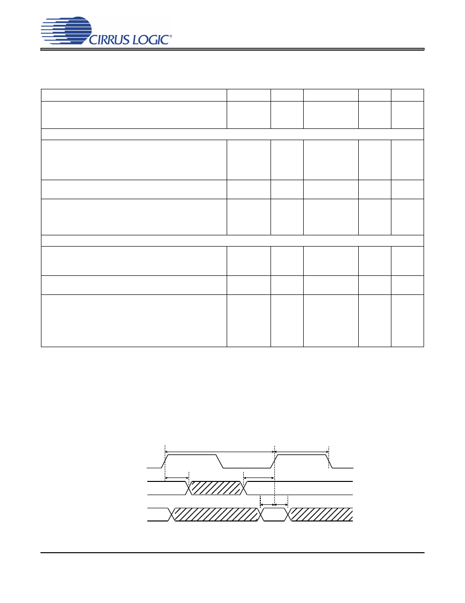
Serial audio interface - i²s/lj timing, Figure 3. i²s/lj timing, Cs5368 serial audio interface - i²s/lj timing – Cirrus Logic CS5368 User Manual
Page 15
DS624F5
15
CS5368
SERIAL AUDIO INTERFACE - I²S/LJ TIMING
The serial audio port is a three-pin interface consisting of SCLK, LRCK and SDOUT.
Logic "0" = GND = 0 V; Logic "1" = VLS; C
L
= 20 pF, timing threshold is 50% of VLS.
Notes:
1. Duty cycle of generated SCLK depends on duty cycle of received MCLK as specified under
.
2. CLKMODE functionality described in
Section 4.6.3 "Master Mode Clock Dividers" on page 24
3. In Slave Mode, the SCLK/LRCK ratio can be set according to preference. However, chip performance
is guaranteed only when using the ratios in
Section 4.7 Master and Slave Clock Frequencies on page
Figure 3. I²S/LJ Timing
Parameter
Symbol
Min
Typ
Max
Unit
Sample Rates
Single-Speed Mode
Double-Speed Mode
Quad-Speed Mode
-
2
54
108
-
54
108
216
kHz
Master Mode
SCLK Frequency
SCLK Period
1/(64*216 kHz)
(CLKMODE = 0)
(CLKMODE = 1)
-
t
PERIOD
t
HIGH
t
HIGH
64*Fs
72.3
40
28
-
-
50
33
64*Fs
-
60
38
Hz
ns
%
%
LRCK setup
before SCLK rising
LRCK hold
after SCLK rising
t
SETUP1
t
HOLD1
20
20
-
-
ns
SDOUT setup
before SCLK rising
SDOUT hold
after SCLK rising (VLS = 1.8 V)
after SCLK rising (VLS = 3.3 V)
after SCLK rising (VLS = 5 V)
t
SETUP2
t
HOLD2
t
HOLD2
t
HOLD2
10
20
10
5
-
-
ns
Slave Mode
SCLK Frequency
SCLK Period
1/(64*216 kHz)
SCLK Duty Cycle
-
t
PERIOD
t
HIGH
-
72.3
28
64*Fs
-
-
-
-
65
Hz
ns
%
LRCK setup
before SCLK rising
LRCK hold
after SCLK rising
t
SETUP1
t
HOLD1
20
20
-
-
ns
SDOUT setup
before SCLK rising (VLS = 1.8 V)
before SCLK rising (VLS = 3.3 V)
before SCLK rising (VLS = 5 V)
SDOUT hold
after SCLK rising (VLS = 1.8 V)
after SCLK rising (VLS = 3.3 V)
after SCLK rising (VLS = 5 V)
t
SETUP2
t
SETUP2
t
SETUP2
t
HOLD2
t
HOLD2
t
HOLD2
4
10
10
20
10
5
-
-
ns
LRCK
SDOUT
SCLK
data
channel
channel
data
t
HOLD2
t
SET UP2
t
HOLD1
t
SET UP1
t
PERIOD
t
HIGH