Cirrus Logic CS44600 User Manual
Channel digital amplifier controller, Features
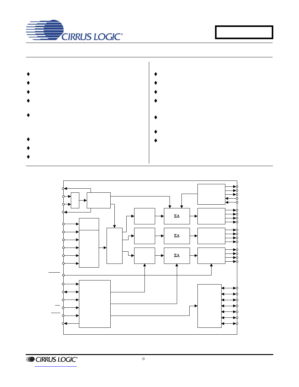
Table of contents
Document Outline
- 1. Characteristics and Specifications
- Specified Operating Conditions
- ABSOLUTE MAXIMUM RATINGS
- DC Electrical Characteristics
- Digital Interface Characteristics
- PWM Output Performance Characteristics
- PWM Filter Characteristics
- Switching Characteristics - XTI
- Switching Characteristics - SYS_CLK
- Switching Characteristics - PWMOUTA1-B3
- Switching Characteristics - PS_SYNC
- Switching Characteristics - DAI Interface
- Switching Characteristics - Control Port - I·C Format
- Switching Characteristics - Control Port - SPI Format
- 2. Pin Descriptions
- 3. Typical Connection Diagrams
- 4. Applications
- 4.1 Overview
- 4.2 Feature Set Summary
- 4.3 Clock Generation
- 4.4 FsIn Clock Domain Modules
- 4.4.1 Digital Audio Input Port
- Table 2. DAI Serial Audio Port Channel Allocations
- Figure 17. I·S Serial Audio Formats
- Figure 18. Left-Justified Serial Audio Formats
- Figure 19. Right-Justified Serial Audio Formats
- Figure 20. One Line Mode #1 Serial Audio Format
- Figure 21. One Line Mode #2 Serial Audio Format
- Figure 22. TDM Mode Serial Audio Format
- 4.4.2 Auto Rate Detect
- 4.4.3 De-Emphasis
- 4.4.1 Digital Audio Input Port
- 4.5 FsOut Clock Domain Modules
- 4.6 Control Port Description and Timing
- 5. Power Supply, Grounding, and PCB layout
- 6. Register Quick Reference
- 7. Register Description
- 7.1 Memory Address Pointer (MAP)
- 7.2 CS44600 I.D. and Revision Register (address 01h) (Read Only)
- 7.3 Clock Configuration and Power Control (address 02h)
- 7.4 PWM Channel Power Down Control (address 03h)
- 7.5 Misc. Configuration (address 04h)
- 7.6 Ramp Configuration (address 05h)
- 7.7 Volume Control Configuration (address 06h)
- 7.8 Master Volume Control - Integer (address 07h)
- 7.9 Master Volume Control - Fraction (address 08h)
- 7.10 Channel XX Volume Control - Integer (addresses 09h - 0Eh)
- 7.11 Channel XX Volume Control1 - Fraction (address 11h)
- 7.12 Channel XX Volume Control2 - Fraction (address 12h)
- 7.13 Channel Mute (address 13h)
- 7.14 Channel Invert (address 14h)
- 7.15 Peak Limiter Control Register (address 15h)
- 7.16 Limiter Attack Rate (address 16h)
- 7.17 Limiter Release Rate (address 17h)
- 7.18 Chnl XX Load Compensation Filter - Coarse Adjust (addresses18h,1Ah,1Ch,1Eh,20h,22h)
- 7.19 Chnl XX Load Compensation Filter - Fine Adjust (addresses19h,1Bh,1Dh,1Fh,21h,23h)
- 7.20 Interrupt Mode Control (address 28h)
- 7.21 Interrupt Mask (address 29h)
- 7.22 Interrupt Status (address 2Ah) (Read Only)
- 7.23 Channel Over Flow Status (address 2Bh) (Read Only)
- 7.24 GPIO Pin In/Out (address 2Ch)
- 7.25 GPIO Pin Polarity/Type (address 2Dh)
- 7.26 GPIO Pin Level/Edge Trigger (address 2Eh)
- 7.27 GPIO Status Register (address 2Fh)
- 7.28 GPIO Interrupt Mask Register (address 30h)
- 7.29 PWM Configuration Register (address 31h)
- 7.30 PWM Minimum Pulse Width Register (address 32h)
- 7.31 PWMOUT Delay Register (address 33h)
- 7.32 PSR and Power Supply Configuration (address 34h)
- 7.33 Decimator Shift/Scale (addresses35h,36h,37h)
- 7.34 Decimator Outd (addresses3Bh,3Ch,3Dh)
- 8. Parameter Definitions
- 9. References
- 10. Package Dimensions
- 11. Thermal Characteristics
- 12. Ordering Information
- 13. Revision History