1 chxx_ovfl, 24 gpio pin in/out (address 2ch), 1 gpio in/out selection (gpiox_i/o) – Cirrus Logic CS44600 User Manual
Page 64: 25 gpio pin polarity/type (address 2dh), 1 gpio polarity/type selection (gpiox_p/t)
64
DS633F1
CS44600
7.23
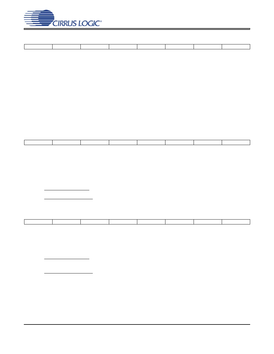
Channel Over Flow Status (address 2Bh) (Read Only)
For all bits in this register, a ‘1’ means the associated condition has occurred at least once since the register
was last read. A ‘0’ means the associated condition has NOT occurred since the last reading of the register.
Reading the register resets all bits to 0 if the Overflow Level/Edge interrupt type is set to “edge trigger”.
These channel overflow status bits are not effected by the interrupt mask bit, M_OVFL_INT. The overflow
condition of each channel can be polled instead of generating an interrupt as required.
7.23.1
ChXX_OVFL
Default = 0
Function:
When high, indicates that the magnitude of the current output sample on the associated channel has ex-
ceeded full scale and has been clipped to positive or negative full scale as appropriate.
7.24
GPIO Pin In/Out (address 2Ch)
7.24.1
GPIO In/Out Selection (GPIOX_I/O)
Default = 0
0 - General Purpose Input
1 - General Purpose Output
Function:
General Purpose Input - The pin is configured as an input.
General Purpose Output - The pin is configured as a general purpose output.
7.25
GPIO Pin Polarity/Type (address 2Dh)
7.25.1
GPIO Polarity/Type Selection (GPIOX_P/T)
Default = 1
Function:
General Purpose Input - If the pin is configured as an input, this bit defines the input polarity (0 = Active
Low, 1 = Active High).
General Purpose Output - If the pin is configured as a general purpose output, this bit defines the GPIO
output type (0 = CMOS, 1 = OPEN-DRAIN).
7
6
5
4
3
2
1
0
RESERVED
RESERVED
CHB3_OVFL
CHA3_OVFL
CHB2_OVFL
CHA2_OVFL
CHB1_OVFL
CHA1_OVFL
7
6
5
4
3
2
1
0
RESERVED
GPIO6_I/O
GPIO5_I/O
GPIO4_I/O
GPIO3_I/O
GPIO2_I/O
GPIO1_I/O
GPIO0_I/O
7
6
5
4
3
2
1
0
RESERVED
GPIO6_P/T
GPIO5_P/T
GPIO4_P/T
GPIO3_P/T
GPIO2_P/T
GPIO1_P/T
GPIO0_P/T