Configuration options, 1 spdif in to headphone or line out, Figure 1. spdif in to headphone or line out – Cirrus Logic CDB43L22 User Manual
Page 8: Figure 1.spdif in to headphone or line out, Fer to, S/pdif in
8
DS792DB1
CDB43L22
3. CONFIGURATION OPTIONS
In order to configure the CDB43L22 for making performance measurements, one needs to use Cirrus Logic’s Win-
dows compatible FlexGUI software to program the various components on the board. This section serves to give a
deeper understanding of the on-board circuitry and the digital clock and data signal routing involved in the different
configuration modes of the CDB43L22. The section also has the expected performance characteristics which are
observed when using the board in the respective configuration mode.
3.1
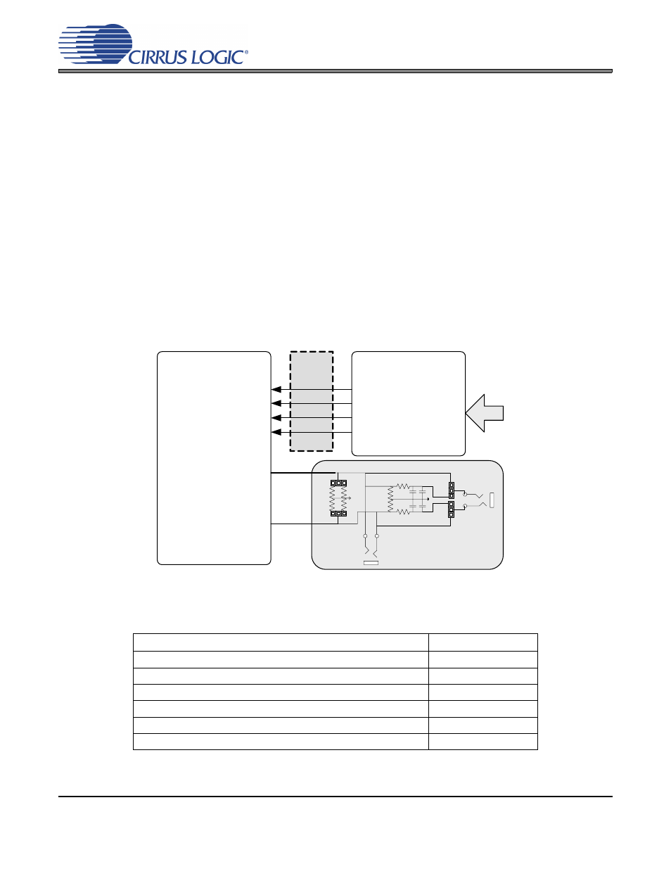
SPDIF In to Headphone or Line Out
The CS43L22’s stereo headphone/line output performance can be tested by loading the “SPDIF In to
Headphone or Line Out” quick setup file provided with the software package. The script configures the
digital clock and data signal routing on the board as shown in
.
Stereo audio outputs can be monitored on the 1/8” jacks J21 or J40. HP jack J21 can be used to connect a
real headphone to provide an actual headphone load while performance measurements are taken on HP
jack J40. Digital S/PDIF input can be provided on the optical (OPT2) or RCA (J68) jacks. Jumpers J8 and
J9 can be used to select output loads and jumpers J1 and J2 can be used to select filtered or unfiltered
outputs. Refer to
for details on software configuration.
Figure 1.
SPDIF In to Headphone or Line Out
shows the expected performance characteristics one should expect when using the CDB43L22 for
SPDIF In to Headphone or Line Out measurements.
Table 1.
SPDIF In to Headphone or Line Out
Performance Plots
Plot
Location
FFT - S/PDIF Input to HP Output @ -1dBFS
FFT - S/PDIF Input to HP Output @ -60dBFS
THD+N vs. HP Output Power
Frequency Response- S/PDIF Input to HP Output @ 0dBFS
THD+N - S/PDIF Input to HP Output
Dynamic Range- S/PDIF Input to HP Output @ -60dBFS
FPGA
CS43L22
CS8416
S/PDIF Rx
RX.RMCK
RX.LRCK
RX.SCLK
RX.SDOUT
S/PDIF
IN
HP/LINE_OUTA
HP/LINE_OUTB
32
Ω
32
Ω
16
Ω
16
Ω
(MASTER)
(SLAVE)
J2
J1
J9
J3
HP
Connect
HP/Line
Output
J40
J21
MCLK
LRCK
SCLK
SDIN