Cirrus Logic CS4382A User Manual
Cs4382a, Features, Description
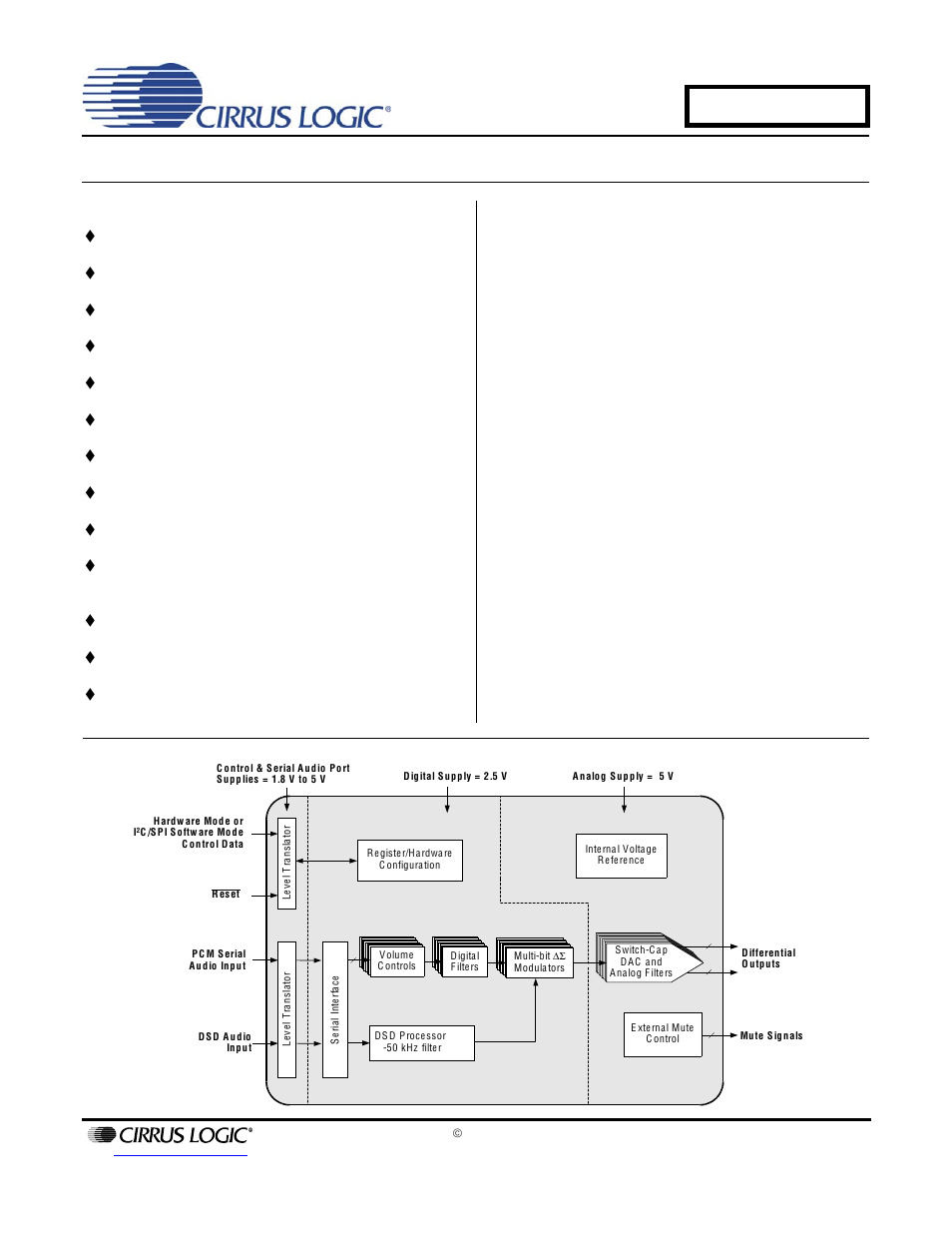
Table of contents
Document Outline
- 1. Pin Description
- 2. Characteristics and Specifications
- Recommended Operating Conditions
- Absolute Maximum Ratings
- DAC Analog Characteristics - Commercial (-CQZ)
- DAC Analog Characteristics - Automotive (-DQZ)
- Power and Thermal Characteristics
- Combined Interpolation & On-Chip Analog Filter Response
- Combined Interpolation & On-Chip Analog Filter Response
- DSD Combined Digital & On-chip Analog Filter Response
- Digital Characteristics
- Switching Characteristics - PCM
- Switching Characteristics - DSD
- Switching Characteristics - Control Port - I·C Format
- Switching Characteristics - Control Port - SPI Format
- 3. Typical Connection Diagram
- 4. Applications
- 4.1 Master Clock
- 4.2 Mode Select
- 4.3 Digital Interface Formats
- 4.4 Oversampling Modes
- 4.5 Interpolation Filter
- 4.6 De-emphasis
- 4.7 ATAPI Specification
- 4.8 Direct Stream Digital (DSD) Mode
- 4.9 Grounding and Power Supply Arrangements
- 4.10 Analog Output and Filtering
- 4.11 Mute Control
- 4.12 Recommended Power-Up Sequence
- 4.13 Recommended Procedure for Switching Operational Modes
- 4.14 Control Port Interface
- 4.15 Memory Address Pointer (MAP)
- 4.16 INCR (Auto Map Increment Enable)
- 5. Register Quick Reference
- 6. Register Description
- 6.1 Mode Control 1 (Address 01h)
- 6.2 Mode Control 2 (Address 02h)
- 6.3 Mode Control 3 (Address 03h)
- 6.4 Filter Control (Address 04h)
- 6.5 Invert Control (Address 05h)
- 6.6 Mixing Control Pair 1 (Channels A1 & B1)(Address 06h) Mixing Control Pair 2 (Channels A2 & B2)(Address 09h) Mixing Control Pair 3 (Channels A3 & B3)(Address 0Ch) Mixing Control Pair 4 (Channels A4 & B4)(Address 0Fh)
- 6.7 Volume Control (Addresses 07h, 08h, 0Ah, 0Bh, 0Dh, 0Eh)
- 6.8 Chip Revision (Address 12h)
- 7. Filter Plots
- 8. Parameter Definitions
- 9. Package Dimensions
- 10. Ordering Information
- 11. References
- 12. Revision History