Digital input characteristics, Power & thermal characteristics, Figure 1. equivalent output test load – Cirrus Logic CS4361 User Manual
Page 8: Figure 2. maximum loading, Figure 2, Ance (see
8
CS4361
Confidential Draft
9/30/11
DIGITAL INPUT CHARACTERISTICS
6.
RST pin has an input threshold relative to VL, but is VA tolerant.
7.
I
in
for LRCK is ±20
A max.
POWER & THERMAL CHARACTERISTICS
8.
Current consumption increases with increasing FS and increasing MCLK. Typ and Max values are
based on highest FS and highest MCLK. Current variance between speed modes is small.
9.
Power-Down Mode is defined when all clock and data lines are held static.
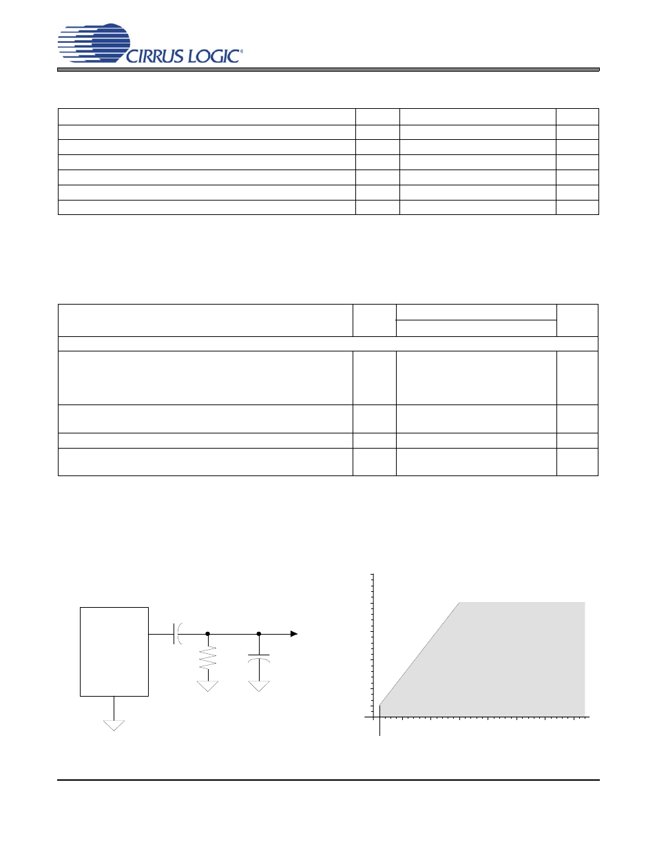
10. Valid with the recommended capacitor values on VQ and FILT+
as shown in the typical connection di-
.
Parameters
Symbol Min
Typ
Max
Units
High-Level Input Voltage -all input Pins except RST (% of VL)
V
IH
70%
-
-
V
Low-Level Input Voltage -all input Pins except RST (% of VL)
V
IL
-
-
30%
V
High-Level Input Voltage -RST pin
(% of VL)
V
IH
90%
-
-
V
Low-Level Input Voltage -RST pin
(% of VL)
V
IL
-
-
10%
V
Input Leakage Current
I
in
-
-
±10
A
Input Capacitance
-
8
-
pF
Parameters
Symbol
5 V Nom
Units
Min
Typ
Max
Power Supplies
Power Supply Current
normal operation
power-down state
I
A
I
L
I
A
I
L
-
-
-
-
66
0.1
300
26
90
1
-
-
mA
mA
A
A
Power Dissipation
normal operation
power-down state
-
-
331
1.63
455
-
mW
mW
Package Thermal Resistance
JA
-
72
-
°C/Watt
Power Supply Rejection Ratio
(1 kHz)
(60 Hz)
PSRR
-
-
60
40
-
-
dB
dB
AO U Tx
AG N D
3.3 µF
V
o ut
R
L
C
L
Figure 1. Equivalent Output Test Load
Figure 2. Maximum Loading
100
50
75
25
2.5
5
10
15
Safe Operating
Region
Cap
a
ci
ti
ve L
o
a
d
--
C
(
p
F
)
L
Resistive Load -- R (k
)
L
125
3
20