Pin descriptions – Cirrus Logic CS4353 User Manual
Page 4
4
DS803F3
CS4353
1. PIN DESCRIPTIONS
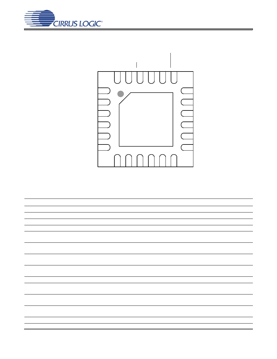
Pin Name Pin #
Pin Description
SCLK
1
Serial Clock (Input) - Serial clock for the serial audio interface.
MCLK
2
Master Clock (Input) - Clock source for the delta-sigma modulator and digital filters.
VL
3
Serial Audio Interface Power (Input) - Positive power for the serial audio interface
DGND
4
Digital Ground (Input) - Ground reference for the digital section.
FLYP+
FLYP-
7
5
Step-up Charge Pump Cap Positive/Negative Nodes (Output) - Positive and Negative nodes for the
step-up charge pump’s flying capacitor.
VCP
6
Charge Pump and Digital Core Logic Power (Input) - Positive power supply for the step-up and invert-
ing charge pumps as well as the digital core logic sections.
VFILT+
8
Step-up Charge Pump Filter Connection (Output) - Power supply from the step-up charge pump that
provides the positive rail for the output amplifiers
FLYN+
FLYN-
9
11
Inverting Charge Pump Cap Positive/Negative Nodes (Output) - Positive and Negative nodes for the
inverting charge pump’s flying capacitor.
CPGND
10
Charge Pump Ground (Input) - Ground reference for the Charge Pump section.
VFILT-
12
Inverting Charge Pump Filter Connection (Output) - Power supply from the inverting charge pump that
provides the negative rail for the output amplifiers.
AOUTB
AOUTA
13
15
Analog Outputs (Output) - The full-scale analog line output level is specified in the Analog Characteris-
tics table.
AOUT_REF
14
Pseudo Diff. Analog Output Reference (Input) - Ground reference for the analog output amplifiers.
This pin must be at the same nominal DC voltage as the AGND pin.
AGND
16
Analog Ground (Input) - Ground reference for the low voltage analog section.
8
7
6
5
4
3
2
1
9
10
11
12
19
20
21
22
23
24
13
14
15
16
17
18
Top-Down (Through Package) View
24-Pin QFN Package
SDIN
LR
CK
I²S
/LJ
DEM
1
_2VRMS
RESET
FLYP+
VFILT+
FL
YN+
CPGND
FL
YN-
SCLK
MCLK
VL
DGND
FLYP-
VBIAS
VA
AGND
AOUT_REF
AOUTB
Thermal Pad
VCP
VFILT-
AOUTA