4 digital interface format, Table 6. digital interface format, Figure 5. i·s, up to 24-bit data – Cirrus Logic CS4353 User Manual
Page 15: Figure 6. left-justified up to 24-bit data, 5 internal high-pass filter, Section 4.4, Cs4353
DS803F3
15
CS4353
4.4
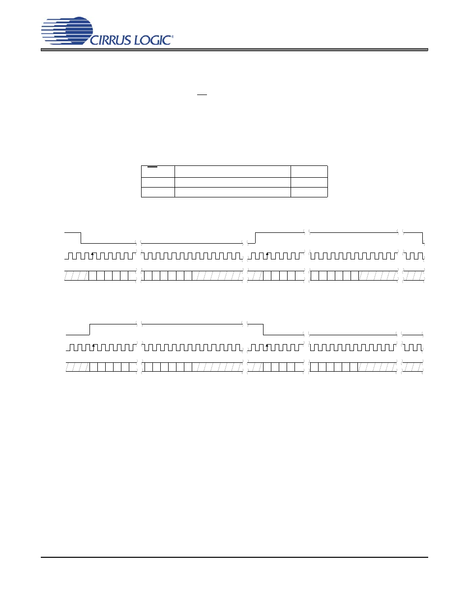
Digital Interface Format
The device will accept audio samples in either I²S or Left-Justified digital interface formats, as illustrated in
The desired format is selected via the I²S/LJ pin. For an illustration of the required relationship between the
LRCK, SCLK and SDIN, see
. For all formats, SDIN is valid on the rising edge of SCLK. Also,
SCLK must have at least 32 cycles per LRCK period in the Left-Justified format.
For more information about serial audio formats, refer to Cirrus Logic Application Note AN282: The 2-Chan-
nel Serial Audio Interface: A Tutorial, available at
Table 6. Digital Interface Format
Figure 5. I²S, up to 24-bit Data
Figure 6. Left-justified up to 24-bit Data
4.5
Internal High-Pass Filter
The device includes an internal digital high-pass filter. This filter prevents a constant digital offset from cre-
ating a DC voltage on the analog output pins. The filter’s corner frequency is well below the audio band; see
the
Combined Interpolation & On-Chip Analog Filter Response
table for filter specifications.
I²S/LJ
Description
Figure
0
I²S, up to 24-bit Data
1
Left-Justified, up to 24-bit Data
LR C K
S C L K
Left C ha nnel
R ig ht C ha nnel
SDIN
+3 +2 +1
+5 +4
M SB
-1 -2 -3 -4 -5
+3 +2 +1
+5 +4
-1 -2 -3 -4
MSB
LSB
LSB
LR C K
S C L K
Left C ha nnel
R ig h t C ha n nel
SDIN
+3 +2 +1
+5 +4
MSB
-1 -2 -3 -4 -5
+3 +2 +1
+5 +4
-1 -2 -3 -4
LSB
M SB
LSB