Cs4299, 2 command address port (slot 1), 3 command data port (slot 2) – Cirrus Logic CS4299 User Manual
Page 15: 4 pcm playback data (slots 3-10)
CS4299
15
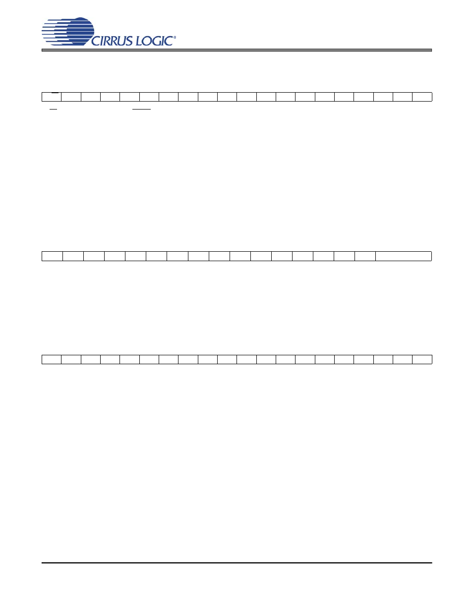
3.1.2
Command Address Port (Slot 1)
R/W Read/Write. When this bit is ‘set’, a read of the AC ’97 register specified by the register index
bits will occur in the AC ’97 2.1 audio codec. When the bit is ‘cleared’, a write will occur. For any
read or write access to occur, the Frame Valid bit (F0) must be ‘set’ and the Codec ID[1:0] bits
(F[14:15]) must match the Codec ID of the AC ’97 2.1 audio codec being accessed. Additionally,
for a primary codec, the Slot 1 Valid bit (F1) must be ‘set’ for a read access and both the Slot 1
Valid bit (F1) and the Slot 2 Valid bit (F2) must be ‘set’ for a write access. For a secondary co-
dec, both the Slot 1 Valid bit (F1) and the Slot 2 Valid bit (F2) must be ‘cleared’ for read and
write accesses. See Figure 9 for bit frame positions.
RI[6:0]
Register Index. The RI[6:0] bits contain the 7-bit register index to the AC ’97 registers in the
CS4299. All registers are defined at word addressable boundaries. The RI0 bit must be ‘clear’
to access CS4299 registers.
3.1.3
Command Data Port (Slot 2)
WD[15:0]
Write Data. The WD[15:0] bits contain the 16-bit value to be written to the register. If an access
is a read, this slot is ignored.
NOTE:
For any write to an AC ’97 register, the write is defined to be an ‘atomic’ access. This means
that when the Slot 1 Valid bit in output Slot 0 is ‘set’, the Slot 2 Valid bit in output slot 0 should
always be ‘set’ during the same audio frame. No write access may be split across 2 frames.
3.1.4
PCM Playback Data (Slots 3-10)
PD[19:0]
Playback Data. The PD[19:0] bits contain the 20-bit PCM playback (2’s complement) data for
the left and right DACs and/or the S/PDIF transmitter. Table 8 on page 30 lists a cross reference
for each function and its respective slot. The mapping of a given slot to a DAC is determined by
the state of the ID[1:0] bits in the Extended Audio ID Register (Index 28h) and by the SM[1:0]
and AMAP bits in the AC Mode Control Register (Index 5Eh).
Bit 19
18
17
16
15
14
13
12
11
10
9
8
7
6
5
4
3
2
1
0
R/W
RI6
RI5
RI4
RI3
RI2
RI1
RI0
0
0
0
0
0
0
0
0
0
0
0
0
Bit 19
18
17
16
15
14
13
12
11
10
9
8
7
6
5
4
3
2
1
0
WD15 WD14 WD13 WD12 WD11 WD10 WD9 WD8 WD7 WD6 WD5 WD4 WD3 WD2 WD1 WD0
Reserved
Bit 19
18
17
16
15
14
13
12
11
10
9
8
7
6
5
4
3
2
1
0
PD19 PD18 PD17 PD16 PD15 PD14 PD13 PD12 PD11 PD10 PD9 PD8 PD7 PD6 PD5 PD4 PD3 PD2 PD1 PD0
DS319PP6
15
CS4299