Cdb4270 – Cirrus Logic CDB4270 User Manual
Page 25
DS686DB3
25
CDB4270
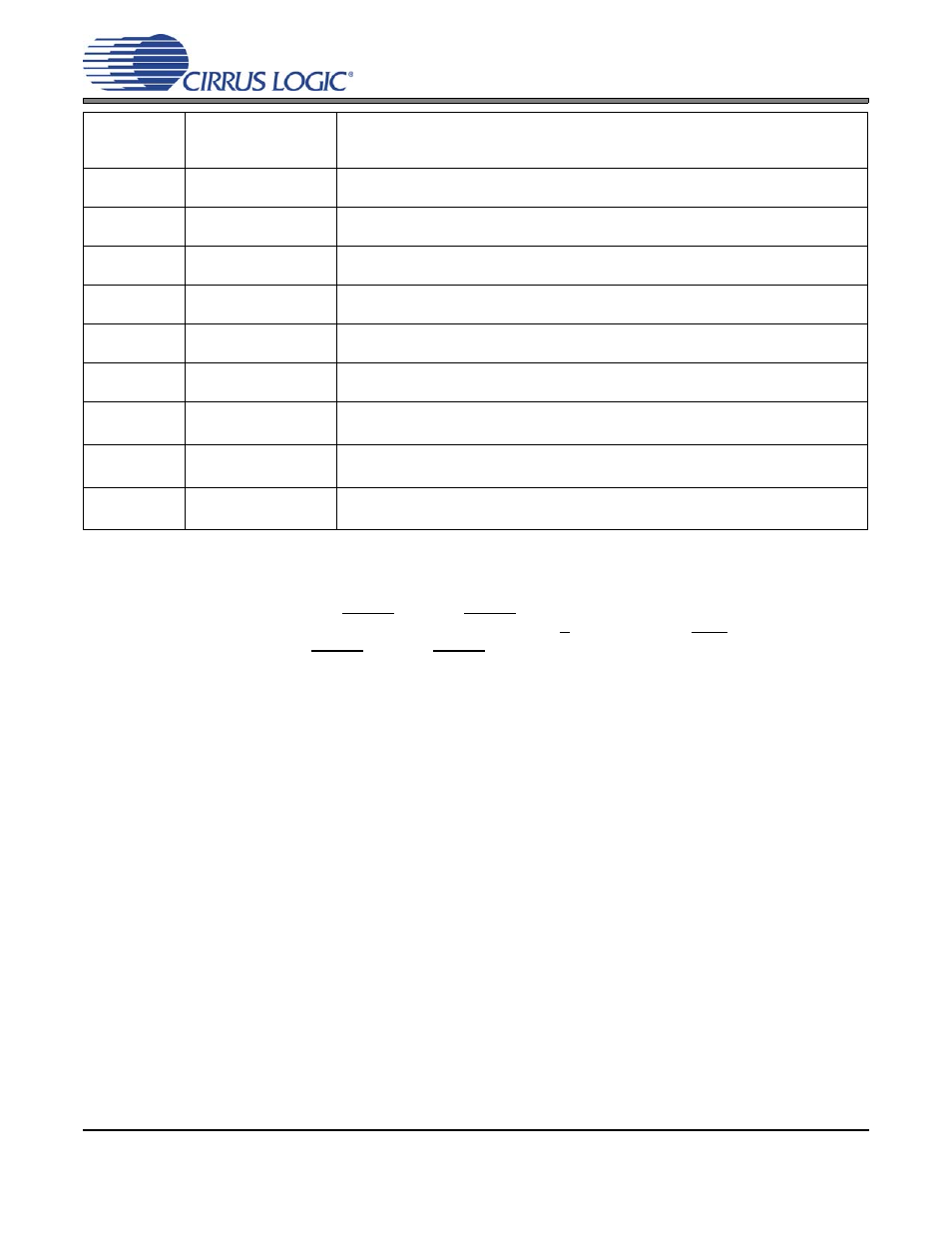
1.
For other M1, M0, MDIV2, MDIV1 states, CS8406 OMCLK=256xFs and CS8416 RMCLK=256xFs.
Note:
Whenever changes are made to the S/PDIF Receiver (CS8416), the FPGA (for CS4270 HW or SW
Modes) generates a CS8416.RESET (CS8416 RESET) after the parameter is changed. Reg 03h (FPGA)
shows the parameters that apply. Also, whenever CS4270-M/S (CS4270 master/slave) changes state, the
FPGA generates a HDR-RESET (CS4270 RESET).
Dip Switch
(1) Logic State
M1, M0, MDIV2,
MDIV1
CS4270 Functional
S2
0,0,0,0
Sets CS4270 Single Speed MCLK divide by 1 Mode, no de-emphasis, CS8406
OMCLK=256xFs and CS8416 RMCLK=256xFs
S2
0,1,0,0
Sets CS4270 Single Speed MCLK divide by 1 Mode, w/de-emphasis, CS8406
OMCLK=256xFs and CS8416 RMCLK=256xFs
S2
1,0,0,0
Sets CS4270 Double Speed MCLK divide by 1 Mode, no de-emphasis, CS8406
OMCLK=128xFs and CS8416 RMCLK=128xFs
S2
1,0,1,0
Sets CS4270 Double Speed MCLK divide by 2 Mode, no de-emphasis, CS8406
OMCLK=256xFs and CS8416 RMCLK=256xFs
S2
1,1,10
Sets CS4270 Quad Speed MCLK divide by 2 Mode, no de-emphasis, CS8406
OMCLK=128xFs and CS8416 RMCLK=128xFs
S2
1,1,1,1
Sets CS4270 Quad Speed MCLK divide by 4 Mode, no de-emphasis, CS8406
OMCLK=256xFs and CS8416 RMCLK=256xFs
Dip Switch
Logic State
DIF net
CS4270 Functional Description
S2
0
Sets CS4270 24-bit LJ Mode for SDIN and SDOUT. CS8406 set to LJ Mode for SDIN
and CS8416 set to LJ Mode for serial data
S2
1
Sets CS4270 24-bit I²S Mode for SDIN and SDOUT. CS8406 set to I²S Mode for
SDIN and CS8416 set to I²S Mode for serial data
Table 13. CDB4270 Hardware Mode - Functional Description