Typical connection diagram, Figure 5. typical connection diagram – Cirrus Logic CS42528 User Manual
Page 19
DS586F2
19
CS42528
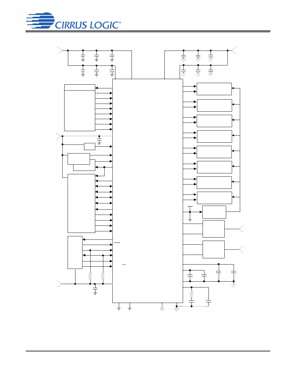
3. TYPICAL CONNECTION DIAGRAM
V D
A O U T A 1+
24
0.1 µF
+
10 µ F
100 µF
0.1 µF
+
+
17
18
V Q
F ILT+
36
37
0.1 µF
4.7 µF
V A
+
10 µ F
51
A O U T A 1-
A O U T B 1+
35
34
A O U T B 1-
A O U T A 2+
32
33
A O U T A 2-
A O U T B 2+
31
30
A O U T B 2-
A O U T A 3+
28
29
A O U T A 3-
A O U T B 3+
27
26
A O U T B 3-
A O U T A 4+
22
23
A O U T A 4-
A O U T B 4+
21
20
A O U T B 4-
M U T E C
38
25
D G N D D G N D
5
R E FG N D
19
41
4
V A
V D
0.1 µF
A G N D
A G N D
52
40
LP F LT
39
A IN L+
A IN L-
A IN R +
A IN R -
15
16
14
13
C onnect D G N D and A G N D at single point near C odec
0.01 µ F
0.1 µF
+
10 µ F
+5 V
0.01 µ F
0.01 µF
+3.3 V to +5 V
+
10 µ F
0.1 µF
0.01 µF
V LS
0.1 µ F
+2.5 V
to +5 V
53
V LC
0.1 µF
+1.8 V
to +5 V
6
3
60
59
62
1
64
61
2
63
8
7
S C L/C C LK
S D A /C D O U T
A D 1/C D IN
R S T
12
9
O M C K
C X _S D IN 1
S A I_LR C K
S A I_S C LK
C X _S D IN 3
C X _S D IN 2
C X _S D IN 4
C X _LR C K
C X _S C LK
A D 0/C S
10
IN T
11
D igital A udio
P rocessor
M icro-
C ontroller
55
R M C K
58
A D C IN 1
57
A D C IN 2
C S 5361
A /D C onverter
C S 5361
A /D C onverter
56
C X _S D O U T
54
S A I_S D O U T
48
46
49
44
45
47
R X P 0
R X P 1/G P O 1
S /P D IF
Interface
50
T X P
D river
U p to 8
S ources
43
R X P 2/G P O 2
R X P 3/G P O 3
R X P 4/G P O 4
R X P 5/G P O 5
R X P 6/G P O 6
R X P 7/G P O 7
42
O S C
A nalog O utput B uffer
2
and
M ute C ircuit (optional)
A nalog O utput B uffer
2
and
M ute C ircuit (optional)
A nalog O utput B uffer
2
and
M ute C ircuit (optional)
A nalog O utput B uffer
2
and
M ute C ircuit (optional)
A nalog O utput B uffer
2
and
M ute C ircuit (optional)
A nalog O utput B uffer
2
and
M ute C ircuit (optional)
A nalog O utput B uffer
2
and
M ute C ircuit (optional)
A nalog O utput B uffer
2
and
M ute C ircuit (optional)
M ute
D rive
(optional)
+V A
*
* P ull up or dow n as
required on startup if the
M ute C ontrol is used.
*
2700 pF *
2700 pF *
Left A nalog Input
R ight A nalog Inpu
A nalog
Input
B uffer
1
A nalog
Input
B uffer
1
C F ILT
3
R F ILT
3
C R IP
3
2 k
2 k
**
**
** R esistors are required for
I
2
C control port operation
1. S ee the A D C Input Filter section in the A ppendix.
2. S ee the D A C O utput Filter section in the A ppendix.
3. S ee the P LL Filter section in the A ppendix.
Figure 5. Typical Connection Diagram
CS42526