Pin descriptions, Pin name # pin description – Cirrus Logic CS42528 User Manual
Page 16
16
DS586F2
CS42528
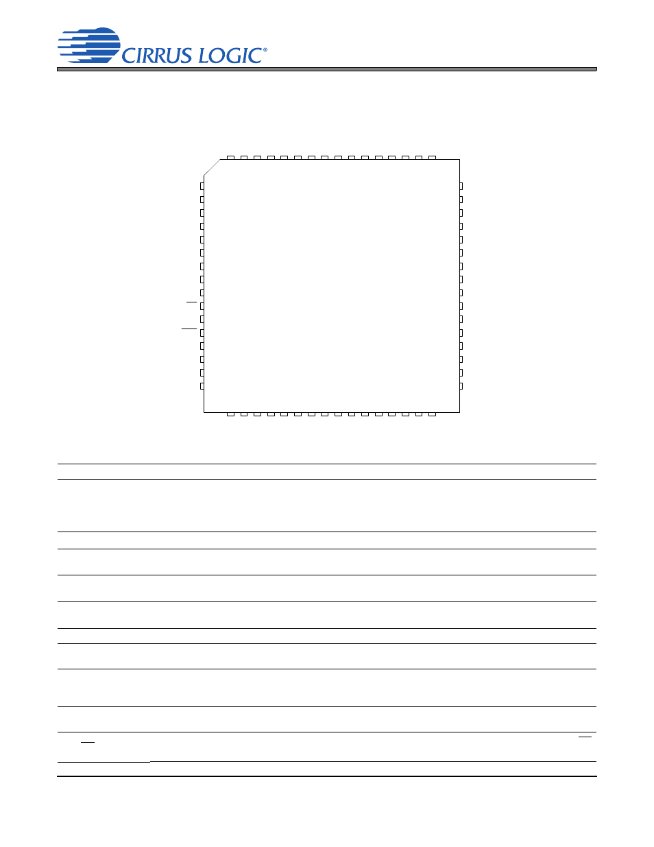
2. PIN DESCRIPTIONS
Pin Name
#
Pin Description
CX_SDIN1
CX_SDIN2
CX_SDIN3
CX_SDIN4
1
64
63
62
Codec Serial Audio Data Input
(Input) - Input for two’s complement serial audio data.
CX_SCLK
2
CODEC Serial Clock
(Input/Output) - Serial clock for the CODEC serial audio interface.
CX_LRCK
3
CODEC Left Right Clock
(Input/Output) - Determines which channel, Left or Right, is currently active on
the CODEC serial audio data line.
VD
4
51
Digital Power
(Input) - Positive power supply for the digital section.
DGND
5
52
Digital Ground
(Input) - Ground reference. Should be connected to digital ground.
VLC
6
Control Port Power
(Input) - Determines the required signal level for the control port.
SCL/CCLK
7
Serial Control Port Clock
(Input) - Serial clock for the serial control port. Requires an external pull-up
resistor to the logic interface voltage in I²C mode as shown in the Typical Connection Diagram.
SDA/CDOUT
8
Serial Control Data
(Input/Output) - SDA is a data I/O line in I²C mode and requires an external pull-up
resistor to the logic interface voltage, as shown in the Typical Connection Diagram. CDOUT is the output
data line for the control port interface in SPI mode.
AD1/CDIN
9
Address Bit 1 (I²C)/Serial Control Data (SPI)
(Input) - AD1 is a chip address pin in I²C mode; CDIN is
the input data line for the control port interface in SPI mode.
AD0/CS
10
Address Bit 0 (I²C)/Control Port Chip Select (SPI) (Input
) - AD0 is a chip address pin in I²C mode; CS
is the chip select signal in SPI mode.
1
2
3
4
5
6
7
8
9
10
11
12
13
14
15
16
17 18 19 20 21 22 23 24 25 26 27 28 29 30 31 32
64 63 62 61 60 59 58 57 56 55 54 53 52 51 50 49
48
47
46
45
44
43
42
41
40
39
38
37
36
35
34
33
CX_SDIN1
SAI
_
S
C
L
K
SAI
_
L
R
C
K
VD
DGND
VLC
SCL/CCLK
SDA/CDOUT
AD1/CDIN
AD0/CS
INT
RST
AINR-
AINR+
AINL+
AINL-
VQ
FI
L
T
+
RE
F
G
ND
AO
U
T
B
4
-
AO
U
T
B
4
+
AO
U
T
A
4
+
AO
UT
A
4
-
VA
AG
N
D
AO
U
T
B
3
-
AO
U
T
B3
+
AO
U
T
A3
+
AO
U
T
A
3
-
AO
UT
B
2
-
AO
U
T
B2
+
AO
U
T
A2
+
AOUTA2-
AOUTB1-
AOUTB1+
AOUTA1+
AOUTA1-
MUTEC
AGND
VARX
RXP7/GPO7
RXP6/GPO6
RXP5/GPO5
RXP4/GPO4
RXP3/GPO3
RXP2/GPO2
RXP1/GPO1
LPFLT
RX
P
0
TXP
VD
DG
ND
VL
S
SAI
_
S
D
O
U
T
RM
CK
CX
_
S
DO
UT
AD
C
IN
2
AD
C
IN
1
OMC
K
CX_LRCK
CX_SCLK
CX
_
S
DI
N4
CX
_
S
DI
N3
C
X
_
S
DI
N2
CS42526