An300 – Cirrus Logic AN300 REV1 User Manual
Page 15

AN300REV1
15
AN300
The circuit illustrates the CS3001 with a gain of negative 408X. Note that the negative output from the bridge is con-
nected to the inverting amplifier input. This results in a positive output from the amplifier into the A/D converter. The
amplifier gain is set by the 71.5K and the parallel combination of the two 350 ohm resistors inside the bridge, or 175
ohm. The 88.7 K resistor offsets the bridge (offset is about +4.9 mV at the minus output side of the bridge) to allow
the input of the A/D to be negative (about -2 V) with no weight on the load cell. The full input span of the A/D is
nominally +/-4 V fully differential, as set by the 5 V on the VREF pin. Adding offset to the bridge output allows use
of the negative range of the A/D and provides more codes out of the converter for the full output span of the bridge
signal. When the full load is applied to the load cell, it will output approximately 5 mV.
The circuit shows the CS5510/12 devices, but the CS5511/13 devices can also be used.
The circuit in
Figure 19
has the disadvantage that when full load is applied to the bridge, the inverting amplifier output
current (2 V / 71.5 k, or about 28 microamperes) must flow through the 71.5 k resistor and into the inverting signal
connection of the bridge. Therefore the inverting side of the bridge sees a different magnitude of current than the
non-inverting side. This imbalance may introduce a signal dependent offset in the bridge due to different tempera-
ture effects on the bridge elements. This can limit the overall accuracy of the measurement.
Figure 20
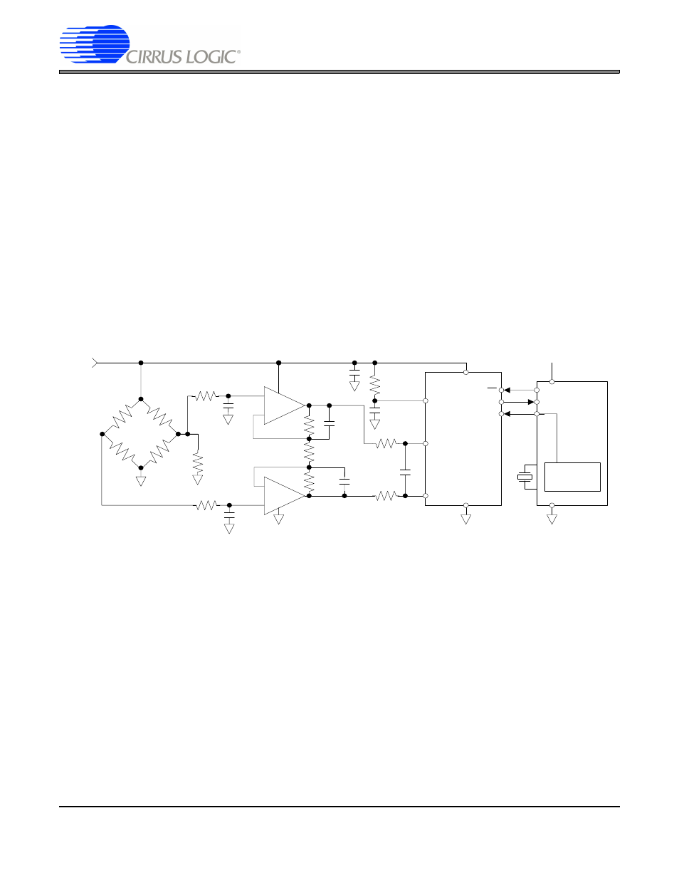
illustrates a different load cell amplifier configuration than
Figure 19
. Using the CS3002, this amplifier con-
figuration yields high impedance to both the plus and minus outputs of the load cell. The high impedance permits
the use of the 1 k
Ω & 300 pF components to prevent the effects of RFI (radio frequency interference).
Figure 20. Digitizer for a Load Cell with High-impedance Inputs
In this schematic, the load cell has a sensitivity of 1 mV/V and outputs only about 5 mV under full load. The sche-
matic illustrates two different gain configurations. If the bridge is used without being offset by resistor R3, the ampli-
fier gain is set for 715X. The output of the amplifier (the input to the A/D) will change from about 0 volts (differential)
to about 3.575 volts (differential) when the load on the load cell goes from zero to full load.
By adding resistor R3, the bridge is offset by about 5 mV. This causes the input to the A/D to be at -3.6 volts (differ-
ential) when no weight is on the scale. The amplifier gain is set for 1419X by changing the value of R1,and produces
a change of about 7.1 volts, differential at the input of the A/D when the load on the load cell changes from zero to
full load. The circuit will achieve about 27,000 noise-free counts on a 5 mV signal.
The noise in this circuit will be limited by the amplifier noise. Changing C1 & C2 to 0.47
µF can increase performance
to about 38,000 noise-free counts. Again, averaging can greatly improve the number of useful counts from the cir-
cuit.
For more information about similar weigh-scale circuits, including some discussion about noise performance, please
refer to Cirrus Logic Application Note AN330, Load Cell Measurement using the CS3001/02/11/12 Amplifiers with
the CS5510/11/12/13 A/D Converters
.
200
Ω
200
Ω
0 .047
µF
VREF
AIN+
AIN-
V-
V+
CS
SDO
SCLK
CS5510/12
µC
+5 V
Counter/Timer
100
Ω
0. 1
µF
+5 V
1 mV/V
-
+
350
Ω
0. 1
µF
140 k
Ω
0.22
µF
CS3002
(86 .6 k
Ω)
-
+
-
+
140 k
Ω
0.22
µF
X 715
(X1419 )
R1
R2
R2
C2
C1
R3
392
Ω
(196
Ω )
300 pF
1 k
Ω
300 pF
1 k
Ω
