Characteristics and specifications, 1 electrical characteristics, Cs1680 – Cirrus Logic CS1680 User Manual
Page 4
CS1680
4
DS1055F1
3. CHARACTERISTICS AND SPECIFICATIONS
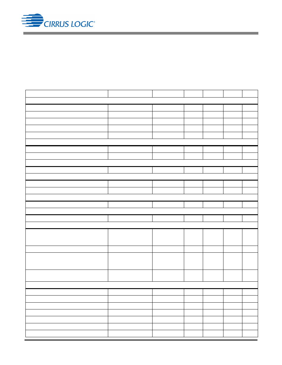
3.1 Electrical Characteristics
Typical characteristics conditions:
- T
A
= 25 °C, V
DD
= 12V, GND = 0 V
- All voltages are measured with respect to GND.
- Unless otherwise specified, all currents are positive when
flowing into the IC.
Minimum/Maximum characteristics conditions:
- T
J
= -40°C to +125 °C, V
DD
= 11V to 17V, GND = 0 V
Parameter
Condition
Symbol
Min
Typ
Max
Unit
VDD Supply Voltage
Operating Range
After Turn-on
V
DD
11
-
17
V
Turn-on Threshold Voltage
V
DD
Increasing
V
ST(th)
-
8.5
-
V
Turn-off Threshold Voltage (UVLO)
V
DD
Decreasing
V
STP(th)
-
7.5
-
V
GPIO Low
V
DD
>
V
ST(th)
K
GPIO(low)
-
50.0
-
%
Zener Voltage
I
DD
= 20mA
V
Z
18.5
-
19.8
V
VDD Supply Current
Startup Supply Current
V
DD
ST(th) I ST - - 1.0 mA Operating Supply Current (Note 3) C L = 0.25nF, f sw 70 kHz - 11 - mA Reference I ref - 64 - A Clamp Gate Drive Z CLAMP(Source) - 290 - Output Sink Resistance Z CLAMP(Sink) - 208 - Boost Output Mode1 Algorithm K Mode1(target) - 73.3 - % Boost Output Mode2 Mode Algorithm K Mode2(target) - 78.4 - % Boost Output Mode3 Algorithm CS1680-00 K Mode3(low) - 60.0 - % Regulation Range High K Mode3(high) - 82.0 - % Accelerated Decrease On CS1680-00 K DEC(on) - 52.2 - % Accelerated Increase On Accelerated Increase Off K CLAMP(on) K CLAMP(off) - 87.8 - % Boost Pulse Width Modulator T1 BST(min) - 0.1 - s Maximum On Time T1 BST(max) - 800 - s Constant Off Time Mode1 T2 BST(fixed) - 0.5 - s Minimum Off Time Mode2 & Mode3 T2 BST(min) - 0.2 - s Maximum Off Time Mode2 & Mode3 T2 BST(max) - 0.9 - s Minimum Switching Frequency - 1.3 - kHz Maximum Switching Frequency - 3.3 - MHz
Reference Current
Output Source Resistance
Regulation Target
Regulation Target
Regulation Range Low
CS1680-02
-
65.9
-
%
CS1680-02
-
60.4
-
%
-
85.1
-
%
Minimum On Time