2 boost stage control, Cs1680 – Cirrus Logic CS1680 User Manual
Page 10
CS1680
10
DS1055F1
boost output voltage continues to fall and reaches the
lowest threshold set by constant K
DEC(on)
, the LED
output current is decreased at an accelerated rate.
If the LED output current I
OUT
is at a maximum and
boost output voltage V
BST
is still above the regulation
high threshold, the controller begins scaling down the
boost inductor current instead of increasing the LED
output current. If this happens, when the boost output
voltage falls below the regulation low threshold, the
boost input current is gradually increased back to
nominal before the LED output current begins to reduce
off from the maximum.
5.3.2 Boost Stage Control
The boost stage uses continuous conduction mode
operation for high compatibility with electronic
transformers. For current regulation, the controller
varies the peak current I
BSTPK
as necessary for dimmer
and transformer compatibility. When the dimmer is
paired with an electronic transformer, period T2
BST
is
modulated to maintain a constant ripple current on the
boost inductor. When the dimmer is paired with a
magnetic transformer, the demagnetization period has
a constant T2
BST(fixed)
time.
Maximum Peak Current
The maximum boost inductor peak current I
BSTPK(max)
is set using the current sense resistor R
BST(Sense)
on
pin BSTSENSE, which is sampled by a comparator
referenced to an internal DAC. Boost peak current
I
BSTPK(max)
is calculated using Equation 1:
Boost overcurrent protection (BOCP) is provided using
a higher threshold to detect the event of inductor
saturation. If the voltage on the BSTSENSE pin
exceeds a threshold voltage V
BSTOCP(th)
of 1.05V, the
controller enters a BOCP fault. The IC output is
disabled, the gate drive output pins BSTGD and
BUCKGD turn off, and the controller attempts to restart
after one second. The boost overcurrent protection
current I
BSTPK(OCP)
is calculated using Equation 2:
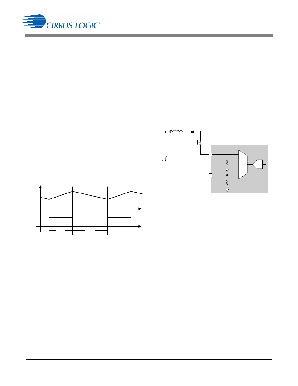
Output BSTOUT Sense and Input VAC Sense
A current proportional to boost output voltage V
BST
is
supplied to the IC on pin BSTOUT and is used as a
control signal (see Figure 11). The ADC is used to
measure the magnitude of current I
BSTOUT
through
resistor R
BST
. The magnitude of current I
BSTOUT
is then
compared to an internal full scale reference current I
ref
of 64
A.
Resistor R
BST
sets the system full-scale voltage and
determines boost output voltage V
BST
regulation, boost
overvoltage protection, and clamp behavior. Full-scale
voltage V
BST(full)
is calculated using Equation 3:
The CS1680-00 is designed for a resistor R
BST
equal to
604k
, creating a full-scale voltage of 40V. The
CS1680-02 is designed for a resistor R
BST
equal to
560k
, creating a full-scale voltage of 37V.
A current proportional to the AC/DC input voltage is
supplied to the IC on pin VAC and is used by the boost
control algorithm.
Dimmer detection and dim level
calculations are dependent on specific levels of the line
voltage. Resistor R
rec
is required to be set equal to
604k
For optimal performance, resistors R
rect
and R
BST
should use 1% or better resistors for best voltage
accuracy.
Boost Overvoltage Protection
The CS1680 supports boost overvoltage protection
(BOP) to protect bulk capacitor C
BST
(see Figure 13 on
T1
BST
i
T2
BST
i
BSTGD
I
L
I
PKBST
I
L
= 0
Figure 10. Continuous Conduction Mode Operation
I
BSTPK max
V
BSTPK th
R
BST Sense
---------------------------------
=
[Eq.1]
I
BSTPK OCP
V
BSTOCP th
R
BST Sense
---------------------------------
=
[Eq.2]
D
B S T
V
rect
V
BST
R
rect
CS1680
I
B S TOUT
BSTOUT
VAC
ADC
I
ref
20k
20k
MUX
15
14
I
V A C
R
B S T
L
B S T
Figure 11. VAC and BSTOUT Input Pin Model
V
BST full
I
ref
R
BST
20k
+
=
[Eq.3]