Introduction, Cs1680, Bucksense – Cirrus Logic CS1680 User Manual
Page 2: Buckzcd, Buckgd vac, Bstout, Clamp, Bstgd, Gpio, Bstsense
CS1680
2
DS1055F1
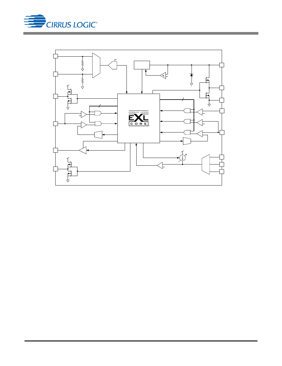
1. INTRODUCTION
A typical schematic using the CS1680 for boost-buck
applications is shown on the previous page.
A startup circuit provides a low-impedance path to
improve electronic transformer compatibility. The GPIO
pin is used to disable the startup circuit when normal
operation is reached.
The CS1680 power supply is connected to an external
power supply network. A linear regulator at the output of
the boost converter provides steady-state operating
current to the IC. The rectified input voltage is sensed as
a current into pin VAC and is used to control the
adaptive transformer and dimmer compatibility
algorithm and extract the phase of the input voltage for
output dimming control.
During steady-state operation, the boost stage operates
in continuous conduction mode (CCM) to boost the
input voltage. This operation allows the boost stage to
provide transformer and dimmer compatibility, reduces
bulk capacitor ripple current, and provides a regulated
input voltage to the buck stage.
The output voltage of the CCM boost is sensed by the
current into the boost output voltage sense pin
(BSTOUT). The buck stage is implemented with
peak-current mode control. Voltage across an external
user-selected resistor is sensed through pin
BUCKSENSE to control the peak current through the
buck stage inductor. Leading-edge blanking on pin
BUCKSENSE prevents false triggering.
When an external negative temperature coefficient
(NTC) thermistor is connected to the eOTP pin, the
CS1680 monitors the system temperature, allowing the
controller to reduce the output current of the system. If
the temperature reaches a designated high set point,
the IC is shutdown and stops switching.
V
Z
POR
+
-
Voltage
Regulator
6
VDD
13
BUCKSENSE
+
-
9
BUCKZCD
+
-
12
BUCKGD
VAC
DAC
+
-
ZCD
4
GND
15
BSTOUT
OCP
11
CLAMP
V
ST(th)
V
STP(th)
V
BUCKOCP(th)
V
BUCKZCD(th)
V
BUCKPK(th)
ADC
I
ref
5
BSTGD
VDD
7
GPIO
3
BSTSENSE
+
-
DAC
+
-
Boost
Peak Ctrl
BOCP
2
V
BSTOCP(th)
V
BSTPK(th)
+
-
I
CONNECT
V
CONNECT
(th)
VDD
Buck
Peak Ctrl
MUX
CTRL2
1
14
eOTP
2
CTRL1
16
20k
20k
MUX
BST Blank
3
Buck Blank
VDD
Figure 1. CS1680 Block Diagram