Solidtron, A1. pulse transformer gating, N-type semiconductor discharge switch, thinpak – Silicon Power CCS SC 14N40_N-Type Semiconductor Discharge Switch, ThinPak User Manual
Page 4
Application Notes
o
V
GE
=15V
T =125
o
C, V
=15V
T =125oC,
V
GE
=15V
T =125
o
C, V
=15V
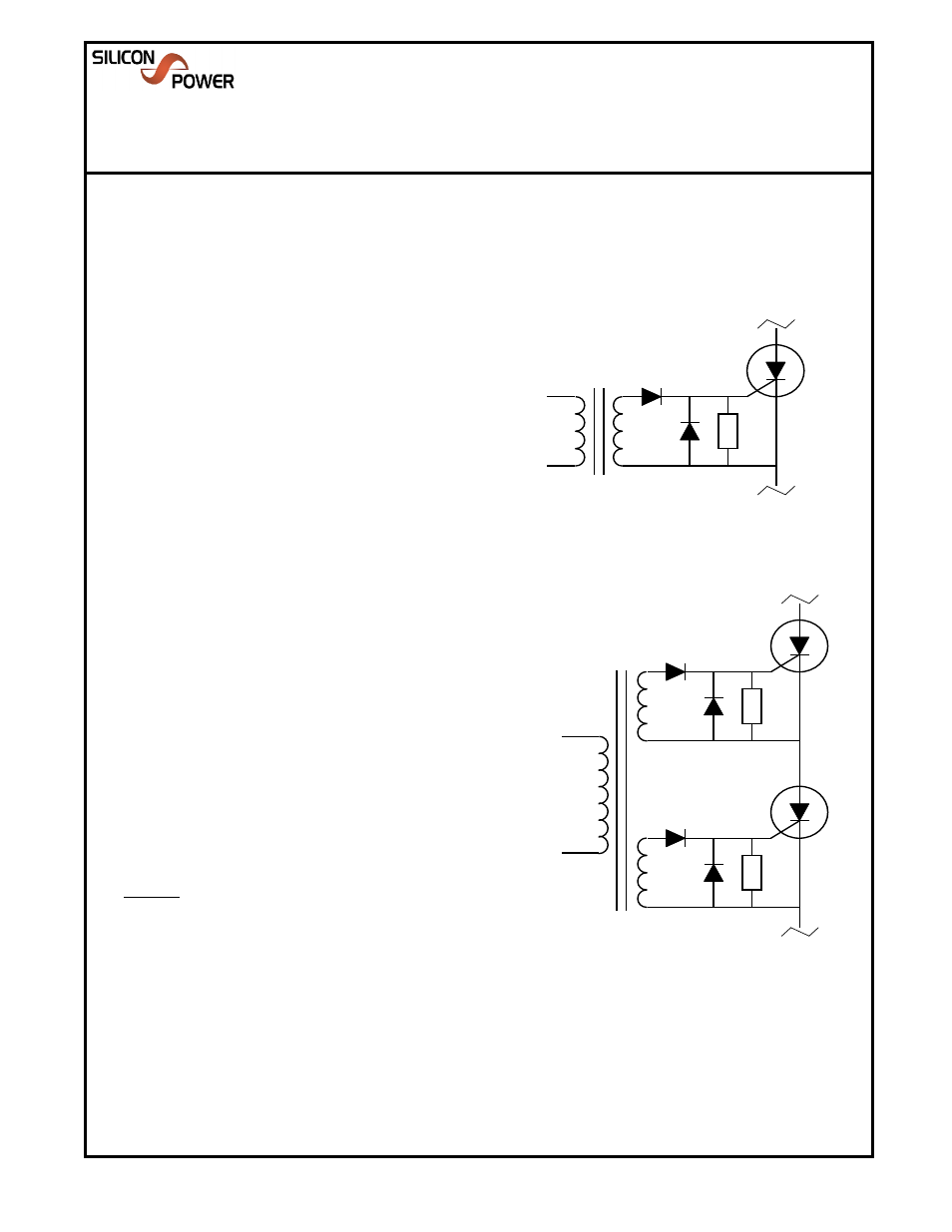
A1. Pulse Transformer Gating
A preferred method of isolation, a pulse transformer may be used to
predictably and reliably trigger the Thyristor. This gating method allows
the user to easily connect the devices in parallel or series (See Fig. A1.2
for series example).
Components (Fig. A1.1)
T
1
- Method of electrically isolating the device from control circuitry.
Pulse X-former insulation characteristic must be selected based on
application requirements.
R
1
(or R
GK
) - Serves as a keep-off resistor, shunting dv/dt induced,
capacitively coupled Anode-Gate current to the Cathode. The lower the
value of R
1
, the better the dv/dt immunity of the sub-circuit. In the event
R
1
must be increased to the point where it's resistance compromises the
dv/dt requirement of the application, a low voltage capacitor (.1-.2uF)
may be placed in parallel to provide a more responsive shunt path;
however, the added capacitance will require more charge be delivered to
satisfy the turn-on requirements outlined in the simplified theory of
operation.
D
1
& D
2
- Current steering diodes. Reverse gate current increases
the impedance of the device ("attempted turn-off"). Reverse gate current
DUT
D
2
D
1
R
1
T
1
Pulse Transformer Gating
ANODE - A
CATHODE - K
S
P
GATE
.7V
Figure A1.1
Basic Pulse X-Former
Gating Circuit
Solidtron
TM
N-Type Semiconductor Discharge Switch,
ThinPak
TM
Data Sheet (Rev 0 - 07/16/08)
CCSSC14N40A10
275 Great Valley Parkway
Malvern, PA 19355
Ph: 610-407-4700
Fax: 610-407-3688
CAO 05/28/09
the impedance of the device ("attempted turn-off"). Reverse gate current
experienced during a high current discharge event may permanently
damage the device. D
1
restricts the direction of current flow through the
secondary while D
2
provides a "free-wheeling" or holding path to the
gate.
It is highly recommended that the components listed above,
specifically R
1
and D
2
be placed in as close physical/electrical proximity
to the device as the application will allow. Parasitic inductance in series
with the Gate to Cathode shunt path will also compromise the dv/dt
immunity of the device.
Theory of Operation (Refer to Fig. A1.1)
A current pulse supplied to the primary of T
1
induces a current into
the secondary of T
1
.
Current supplied by the T
1
secondary forward
biases D
1
supplying current through R
1
; thus, developing voltage across
R
1
until the gate of the Thyristor is forward biased (~0.7V).
Current is
then supplied to the Gate of the Thyristor until turn-on (latched-on) is
achieved.
Following the discharge event, once the Thyristor current
reaches zero and it's stored charge is cleared (Storage Time) the circuit
is reset and Anode voltage may be reapplied.
Example:
Turn-on will occur with R
1
=5 ohms, I
T1-S
=/> 140mA
It is recommended that T
1
secondary current (I
T1-S
) =/> 0.7V / R
1
be
supplied for approximately 2uSec.
Device turn-on delay (T
D-ON
) is
typically less than 200nSec.
Although I
T1-S
= 0.7V / R
1
is sufficient to turn the device on, we
typically recommend, where possible,
I
T1-S
=/ >500mA, Pulse Duration
=/> 5uSec with R
1
= 10 ohms.
D
2
D
1
R
1
D
2
D
1
R
1
T
1
Figure A1.2
Series Connection
Pulse X-Former Gating
CAO 05/28/09